Photoresist supply apparatus and method of controlling the operation thereof

a technology of photoresist and supply apparatus, which is applied in the direction of superimposed coating process, liquid/solution decomposition chemical coating, instruments, etc., can solve the problems of process defects and waste of operation, and achieve the effect of preventing an unnecessary consumption of photoresis

Inactive Publication Date: 2005-03-31
SAMSUNG ELECTRONICS CO LTD
View PDF6 Cites 12 Cited by
  • Summary
  • Abstract
  • Description
  • Claims
  • Application Information

AI Technical Summary

Benefits of technology

[0019] Accordingly, an object of the present invention is to provide a photoresist supply apparatus capable of preventi

Problems solved by technology

This operation can be wasteful because various amounts of the photoresist, determined by each worker, are discharged during the filling of the tra

Method used


Image

  • Photoresist supply apparatus and method of controlling the operation thereof
  • Photoresist supply apparatus and method of controlling the operation thereof
  • Photoresist supply apparatus and method of controlling the operation thereof

Examples


Embodiment Construction

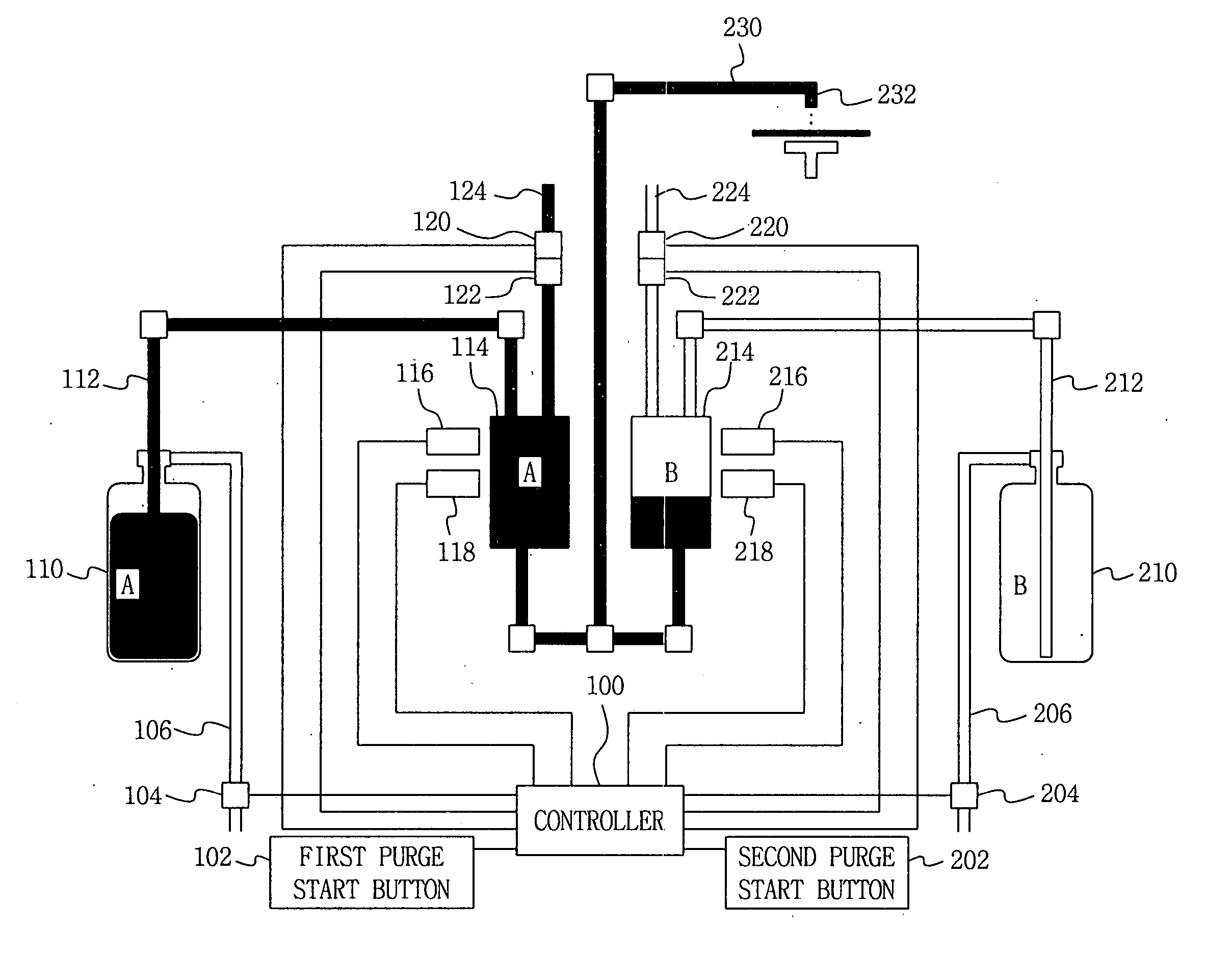
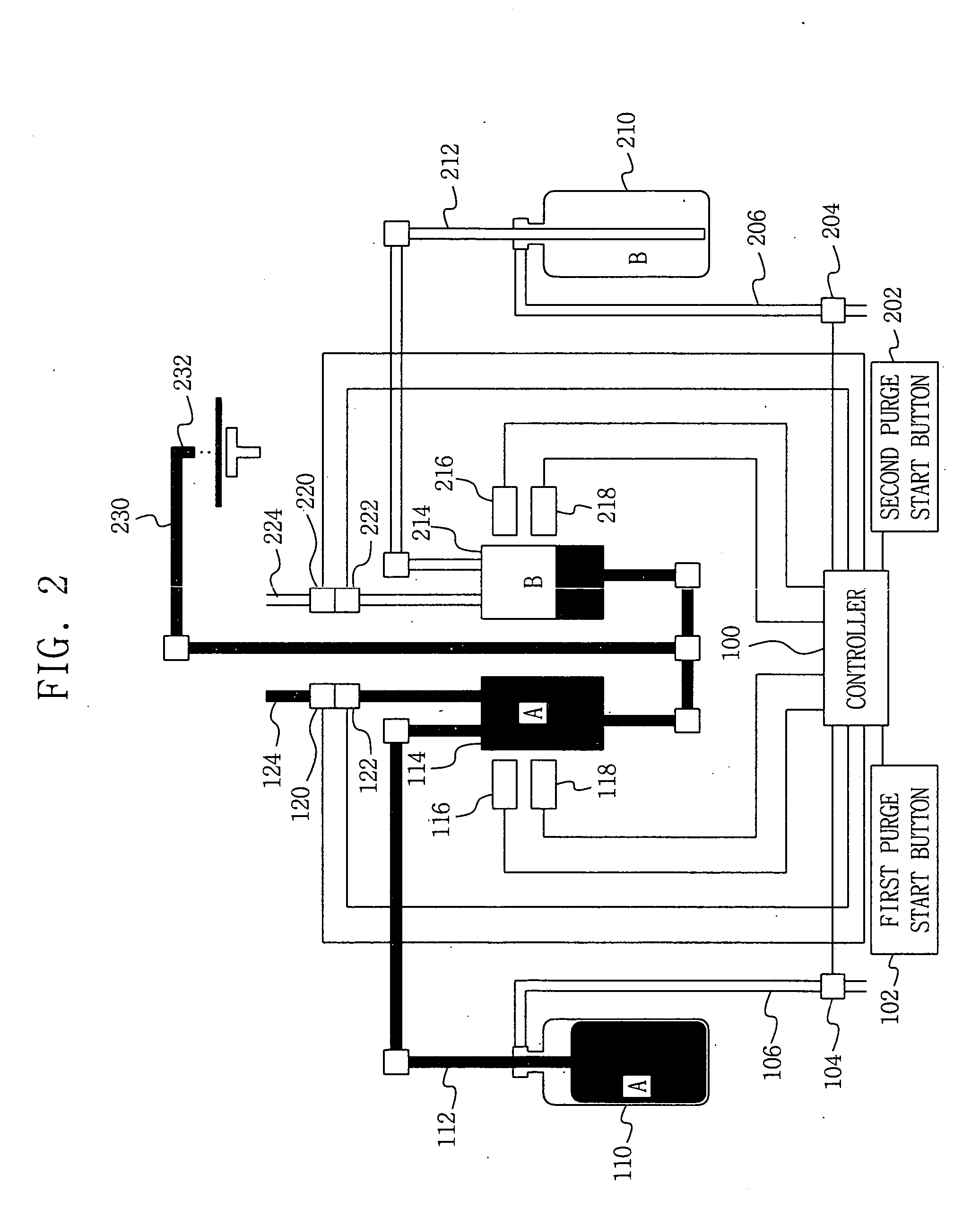
[0037] The present invention will now be described in detail with reference to FIGS. 2, 3A and 3B. For the sake of clarity, though, a detailed description of known functions and systems has been omitted.

[0038] Referring first to FIG. 2, a photoresist supply apparatus for use in semiconductor coating equipment according to the present invention includes first and second photoresist bottles 110 and 210, first and second gas supply pipes 106 and 206, first and second solenoid valves 104 and 204, first and second purge start buttons 102 and 202, first and second photoresist supply pipes 112 and 212, first and second trap tanks 114 and 214, a third photoresist supply pipe 230, a nozzle 232, first and second level sensors 116 and 216, third and fourth level sensors 118 and 218, first and second discharge pipes 124 and 224, third and fourth solenoid valves 120 and 220, first and second drain sensors 122 and 222, and a controller 100.

[0039] The first and second photoresist bottles 110 and...


PUM


Abstract

A photoresist supply apparatus of semiconductor coating equipment fills a supply line with new photoresist when a used photoresist bottle is replaced. The photoresist supply apparatus includes first and second photoresist bottles, first and second gas supply pipes connected to the bottles, first and second solenoid valves disposed along the gas supply pipes, first and second purge start buttons, first and second photoresist supply pipes, first and second trap tanks to which the supply pipes are connected, a third photoresist supply pipe connected to the trap tanks, a nozzle connected to the third photoresist supply pipe, first and second level sensors disposed at an upper level of the trap tanks, third and fourth level sensors disposed at a lower level of the trap tank, first and second discharge pipes connected to the trap tanks, third and fourth solenoid valves disposed along the discharge pipes, first and second drain sensors associated with the discharge pipes, and a controller.

Description

BACKGROUND OF THE INVENTION [0001] 1. Field of the Invention [0002] The present invention relates to semiconductor coating equipment. More particularly, the present invention relates to photoresist supply apparatus for dispensing photoresist onto a substrate such as a semiconductor wafer. [0003] 2. Description of the Related Art [0004] The processes involved in the manufacturing of semiconductor devices can be generally classified as fabrication, assembly and test processes. The fabrication processes include supply, diffusion, photolithography, etching and thin film-forming processes. These processes are carried out selectively and repeatedly on a wafer to construct an electrical circuit on the wafer. [0005] In the photolithography process, an oxide film is formed on the surface of a polished silicon wafer to protect a surface of the wafer, liquid photoresist is dispensed onto the oxide film, and then the wafer is rotated at a high speed to form a uniform coating of the photoresist ...

Claims


Application Information

Patent Timeline
IPC IPC(8): H01L21/027B05D1/00G03F7/16H01L21/00
CPCG03F7/162H01L21/67253H01L21/6715H01L21/027
Inventor KIM, YONG-KYUNG
Owner SAMSUNG ELECTRONICS CO LTD
Why Eureka
Try Eureka