

Method of charged particle beam lithography and equipment for charged particle beam lithography
a technology of charged particle beams and equipment, applied in the field of semiconductor manufacturing technology, to achieve the effect of maximizing the number and not degrading the accuracy of exposur
- Summary
- Abstract
- Description
- Claims
- Application Information
AI Technical Summary
Benefits of technology
Problems solved by technology
Method used
Image

Examples
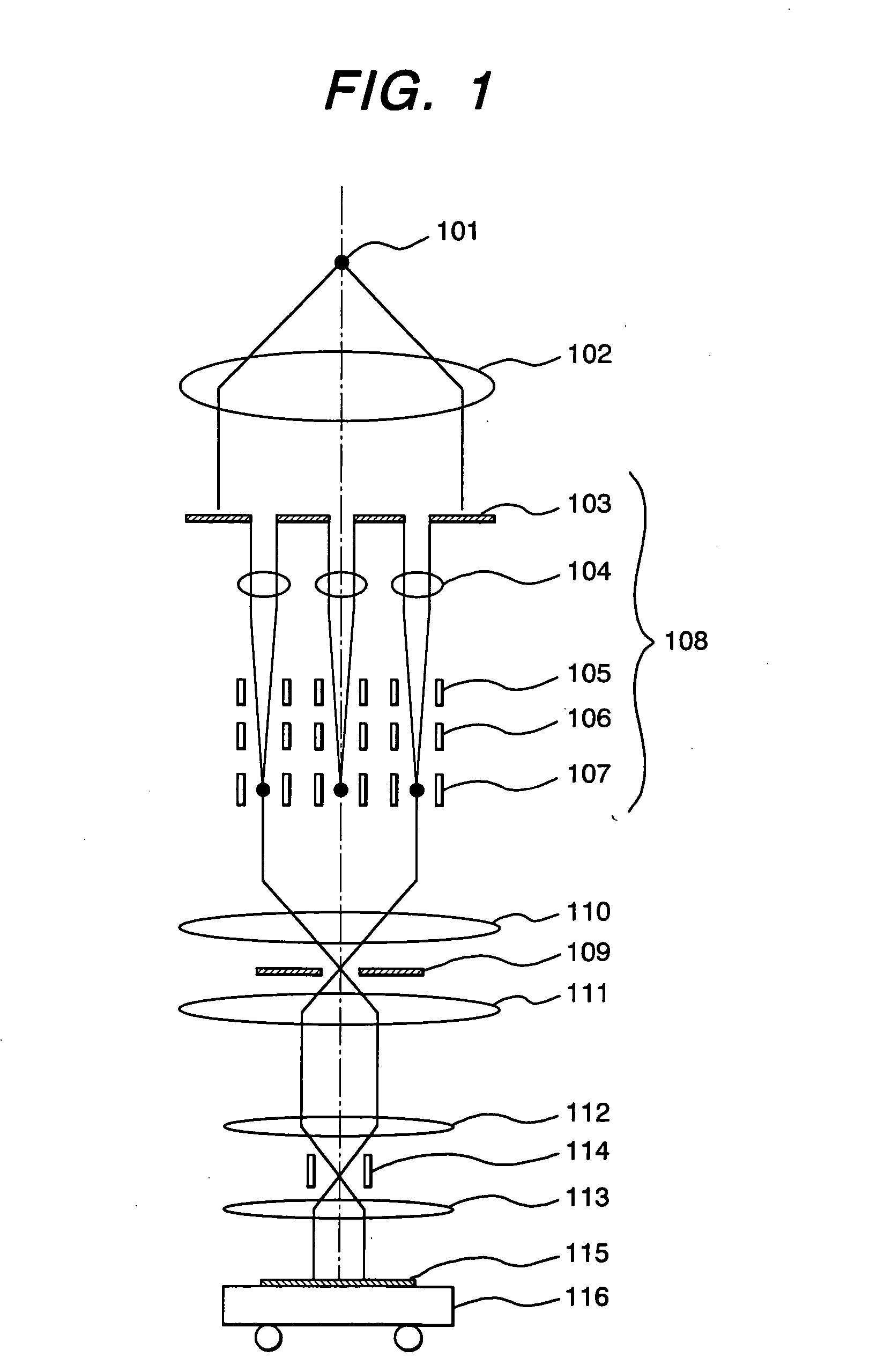
first embodiment
[0108] (First Embodiment)
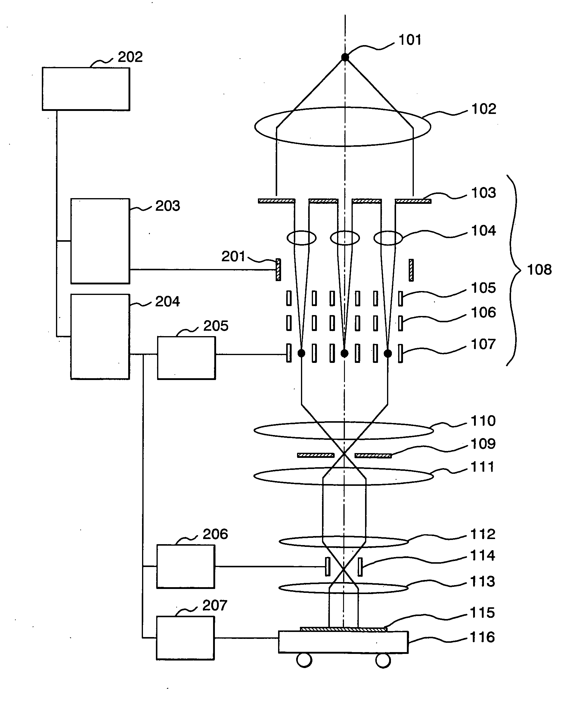
[0109]FIG. 2 shows the structure of a multibeam type electron beam exposure apparatus according to the first embodiment of the invention.
[0110] As mentioned earlier, such a multibeam system demands that irradiation and non-irradiation of all of a plurality of electron beams to be used for exposure onto a sample should be well controlled and the electron beams should be well converged at a desired position. A failure or so of a multibeam forming device may cause the following problems on an electron beam to be formed.
[0111] (1) A specific beam is unable to reach a sample.
[0112] This is a case, for example, where a foreign matter is adhered to the trajectory of an electron beam, or where the path of an electron beam is diverted by the disturbance of an electromagnetic field. At this time, an exposed pattern is partly dropped off or grazed.
[0113] (2) The property of a specific beam is degraded.
[0114] This is a case, for example, where of lenses constitutin...
second embodiment
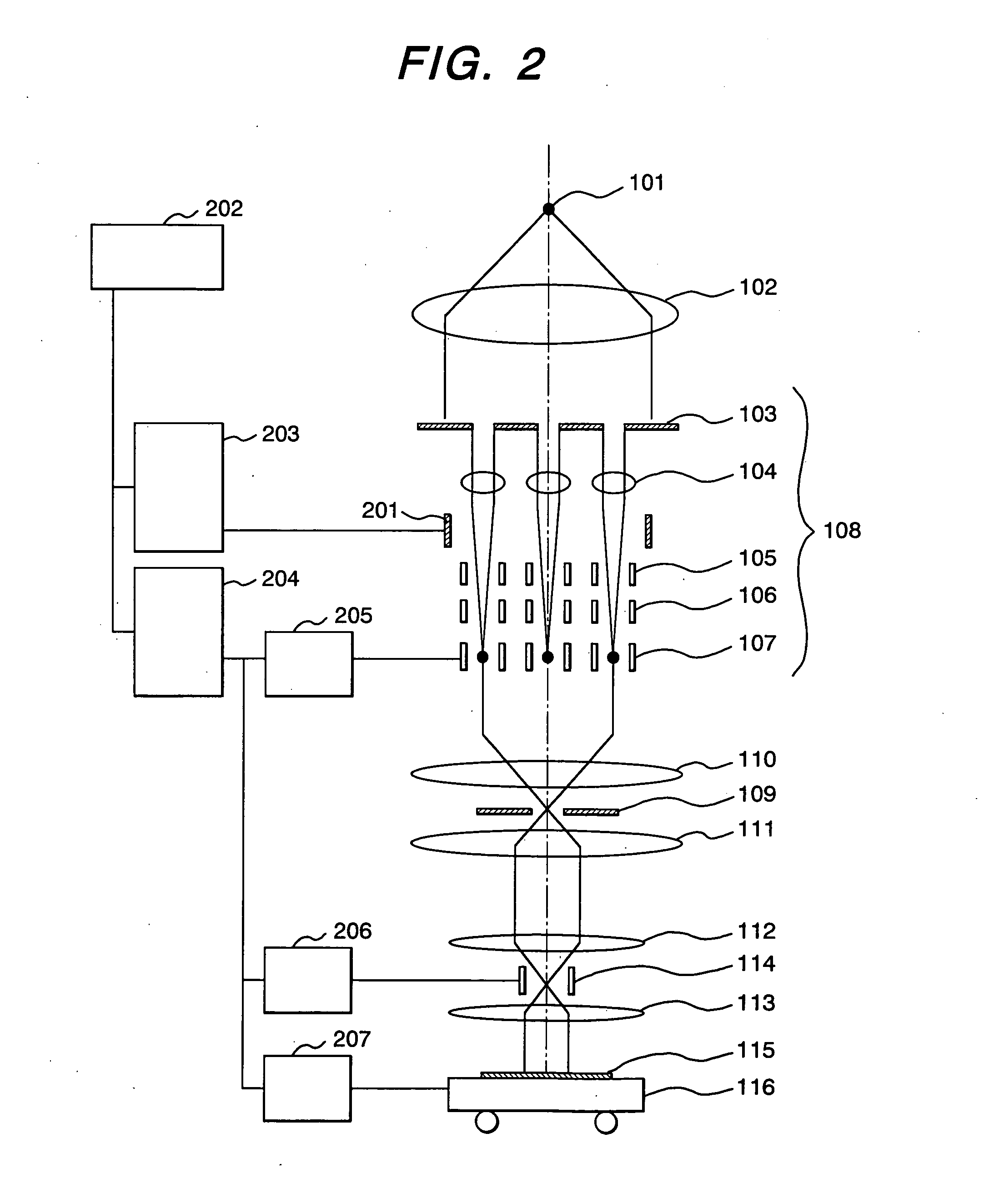
[0161] (Second Embodiment)
[0162] The second embodiment of the invention blocks defective electron beams to a sample and performs an exposure process by using only good beams without changing the mode of the multibeam type electron beam exposure apparatus shown in FIG. 1, while coping with bad properties of beams originated from failures or so in multibeam forming devices like those which are handled in the first embodiment.
[0163] In the embodiment, deflector arrays 105 and 106 in FIG. 1 are used to block beams with bad properties. As described in the “BACKGROUND OF THE INVENTION”, the deflector array should originally work to deflect passing electron beams to individually adjust the positions of intermediate images of electron sources formed on the blanker array 107 in a plane orthogonal to the optical axis. In the embodiment, however, when a failure occurs in the blanker array and a specific electron beam cannot be blocked to a sample, the deflector array is used as a blanker the ...
third embodiment
[0172] (Third Embodiment)
[0173]FIG. 7 shows the structure of a multibeam type electron beam exposure apparatus according to the third embodiment of the invention.
[0174] In the embodiment, a movable shutter 701 is provided on the beam trajectory, specifically, between the aperture array 103 and the lens array 104. The aperture of the movable shutter 701 has an approximately square shape large enough to be able to pass all of M×N beams split by the aperture array 103 at the height (z) of the movable shutter 701. With the z direction being the beam traveling direction, the movable shutter 701 can move within a plane approximately perpendicular to the z direction.
[0175] Adjusting the position of the movable shutter 701 within the xy plane can allow some (m×n) or all of the beams split by the aperture array 103 to reach the sample and block the remaining beams. That is, it is possible to block beams with bad properties and extract only beams with good properties.
[0176] The performance...
PUM
| Property | Measurement | Unit |
|---|---|---|
| size | aaaaa | aaaaa |
| area | aaaaa | aaaaa |
| shape | aaaaa | aaaaa |
Abstract
Description
Claims
Application Information