Lightemitting device and method of manufacturing the same

a technology of light emitting device and manufacturing method, which is applied in the direction of solid-state devices, semiconductor devices, lighting and heating apparatus, etc., can solve the problems of short life time and high power consumption, heat dissipation of led and extracting light efficiency, and light output may decrease, so as to achieve high light reflection efficiency

Inactive Publication Date: 2005-04-07
NICHIA CORP
View PDF4 Cites 116 Cited by
  • Summary
  • Abstract
  • Description
  • Claims
  • Application Information

AI Technical Summary

Benefits of technology

[0019] This method enables it to obtain the light emitting device capable of increasing the proportion of light that can be used as a light source to the total light emitted by the LED chip. That is, it

Problems solved by technology

Fluorescent lamps and incandescent lamps are currently used as ordinary light sources, and they have short life times and high power consumption.
Problems that arise when LED is used as a light source are heat dissipation of the LED and the efficiency of extracting light.
When heat is not dissipated efficiently from the LED apparatus, light output may decrease and/or life time of the LED may become shorter due to the heat applied to the LED.
However, since the resin substrate 14 has a low heat conductivity and provides poor heat dissipation through the side face of the recess, the LED mounting substrate tends to overheat.
As a result, the sealing member, the adhesive and the other components deteriorate and the luminance of light emission decreases.
Such problems become more conspicuous when a plurality of LEDs are mounted for the purpose of increasing the light output

Method used


Image

  • Lightemitting device and method of manufacturing the same
  • Lightemitting device and method of manufacturing the same
  • Lightemitting device and method of manufacturing the same

Examples


example 1

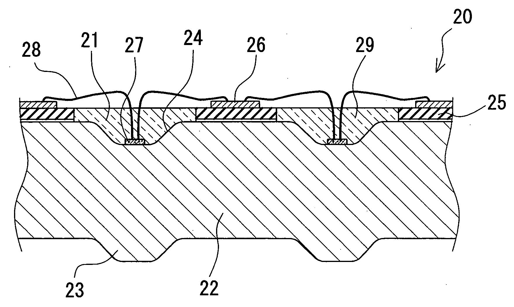
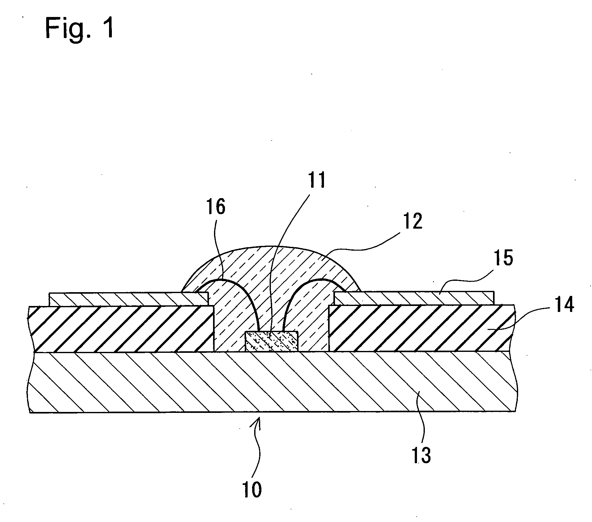
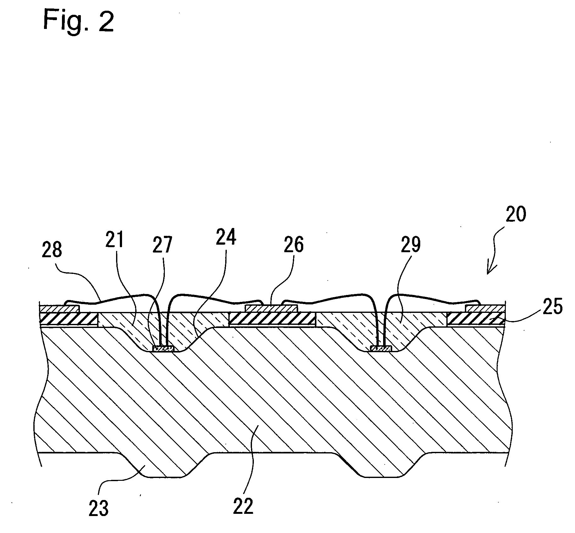
[0056]FIG. 3 is a plan view schematically showing a LED mounting substrate for light source of the present invention having LED mounted thereon in one example. FIG. 4 is a sectional view taken along lines A-A′ of FIG. 3. The LED mounting substrate for light source of the present invention is made in such a configuration as the recess formed in the metallic mounting substrate 22 becomes wider toward the opening as shown in FIG. 2, where the light reflecting layer 24 consists of metal layers formed on the side face of the recess and on the bottom surface, and the electrically conductive member 26 is provided via the insulating member 25. When the LED mounting substrate for light source of the present invention is used as shown in FIG. 3, it is preferable to form a plurality of recesses 21 on the same plane and place a plurality of LEDs therein. The mounting substrate having the plurality of LEDs mounted thereon makes it possible to obtain a level of brightness comparable to that of th...

example 2

[0062] While one LED was placed in one recess in Example 1, a plurality of LEDs may also be placed in one recess. For example, LEDs that emit three primary colors, blue (B), green (G) and red (R) may be placed in a recess. In such a constitution, light emitted by the LED chip is reflected on the inner surface of the light reflecting layer and is directed forward in front of the light emitting device, thereby improving the luminance of light emission and sufficiently mixing the light emitted by the LEDs within the recess.

example 3

[0063] In Example 1 and Example 2, the insulating member having the through holes is bonded onto the metal plate with the insulating adhesive and the electrically conductive members are provided on the insulating member, after forming the recess on the upper surface of the metal plate and the projection on the component mounting surface and forming the light reflecting layer. However, the metallic mounting substrate may also be made by preparing a substrate whereon an insulating layer is formed on the upper surface of an ordinary metallic substrate, namely a metal plate, and an electrically conductive layer is formed on the insulating layer. The ordinary metallic substrate is formed, for example, by bonding the insulating layer and the electrically conductive layer on the metal plate with an insulating adhesive. The metal plate, the insulating member and the electrically conductive member are made of the same materials as those of the metal plate, the insulating member and the elect...


PUM


Abstract

A light emitting apparatus includes a metallic substrate having at least one recess on the surface and at least one projection opposing the recess on the back surface thereof, a light emitting element mounted in the recess of the metallic substrate, the light emitting element having a pair of positive and negative electrodes formed on one side thereof, and electrically conductive members formed via an insulating member on the surface of the metallic substrate, the electrically conductive members being electrically connected with the pair of positive and negative electrodes of the light emitting element.

Description

TECHNICAL FIELD [0001] The present invention relates to a light emitting device comprising a semiconductor element mounted on a mounting substrate, and particularly to a light emitting device that provides a light source having high luminance by using a metallic substrate having recess formed therein as the mounting substrate and providing a light reflecting layer on side face of the recess. BACKGROUND ART [0002] Fluorescent lamps and incandescent lamps are currently used as ordinary light sources, and they have short life times and high power consumption. LED, when used as a light source, has a longer life time and lower power consumption. Thus LED is viewed as promising for use as a light source that replaces fluorescent lamp and the like. [0003] Problems that arise when LED is used as a light source are heat dissipation of the LED and the efficiency of extracting light. When heat is not dissipated efficiently from the LED apparatus, light output may decrease and / or life time of t...

Claims


Application Information

Patent Timeline
IPC IPC(8): H01L25/075H01L33/64
CPCH01L25/0753H01L33/64H01L33/641H01L33/642H01L2224/45144H01L2224/48091H01L2924/00014H01L2924/00
Inventor TAKINE, KENJI
Owner NICHIA CORP
Why Eureka
Try Eureka