
Semiconductor device and a method for fabricating the semiconductor device

a semiconductor and device technology, applied in the direction of semiconductor devices, basic electric elements, electrical equipment, etc., can solve the problems of dramatically increasing the junction resistance of the source per cell and much greater, and achieve the effect of reducing the resistan

Inactive Publication Date: 2005-04-07
DONGBU ELECTRONICS CO LTD
View PDF3 Cites 195 Cited by
  • Summary
  • Abstract
  • Description
  • Claims
  • Application Information

AI Technical Summary

Benefits of technology

[0009] It is therefore desirable to address the above problem and to provide a method for fabricating a semiconductor device, which is capable of reducing the resistance generated from adopting the SAS technique.
[0010] It is also desirable to provide a method for fabricating a semiconductor device, which is capable of reducing the resistance at the sidewall of the SAS region.

Problems solved by technology

However, the conventional SAS technique has a drawback in that junction resistance of the source per cell dramatically increases because the SAS region is formed along a trench profile.
Moreover, the SAS technique has another drawback in that the resistivity at a sidewall of a trench, which is a boundary region between the trench region and an active region, is much greater than and may be about 10 times as much as that at the horizontal surfaces of the trench, because the depth and amount of the implantation of the impurity ions in the sidewall are smaller than those in the other regions, such as the horizontal surfaces of the trench and the active regions.

Method used


Image

  • Semiconductor device and a method for fabricating the semiconductor device
  • Semiconductor device and a method for fabricating the semiconductor device
  • Semiconductor device and a method for fabricating the semiconductor device

Examples


Embodiment Construction

[0026] Reference will now be made in detail to exemplary embodiments of the invention, examples of which are illustrated in the accompanying drawings. Wherever possible, the same reference numbers will be used throughout the drawings to refer to the same or like parts.

[0027] The SAS technique is a technology for reducing the size of a memory cell in a bit line direction by decreasing a gap between a gate and a source of transistors. The SAS technique is an essential process for devices with a below−0.25 μm line width.

[0028] Typically, a NOR type flash memory utilizes a common source and one source contact is formed per 16 memory cells.

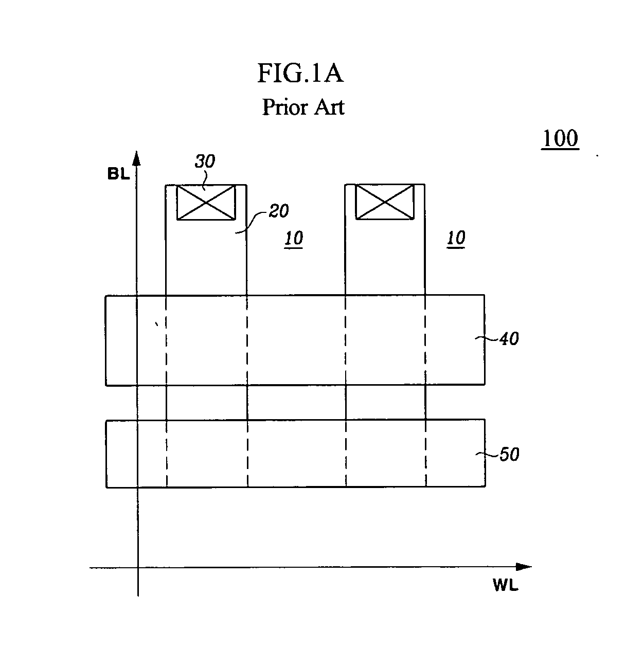
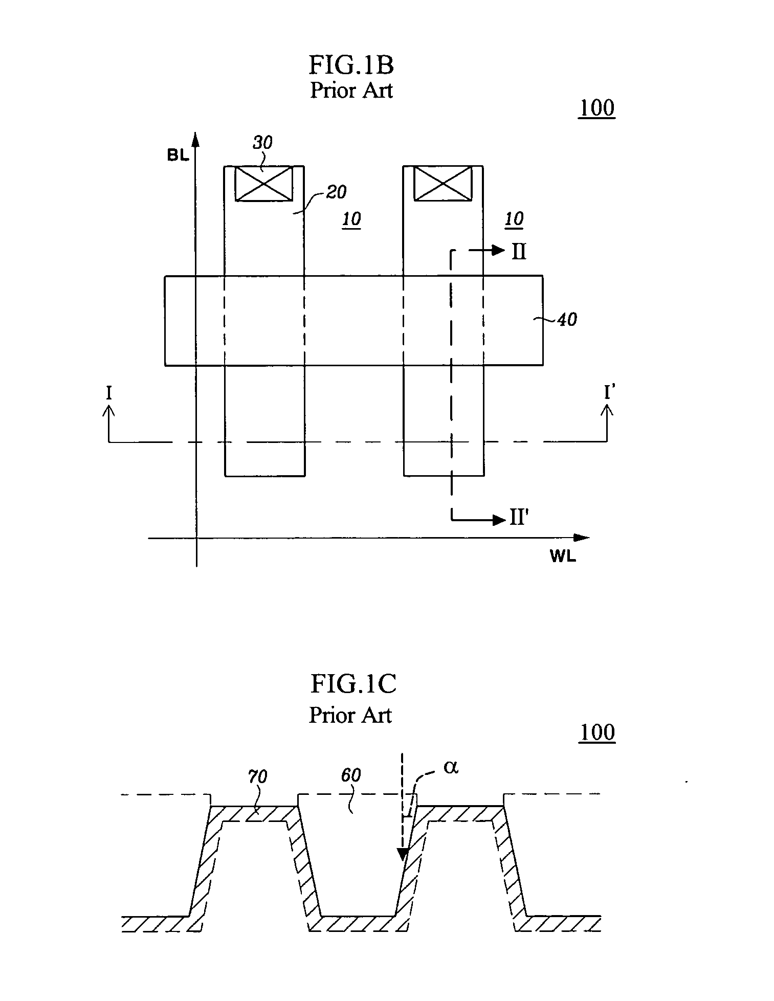
[0029]FIG. 1A is a plan view illustrating a conventional memory cell 100 without using the SAS technique, FIG. 1B is a plan view illustrating memory cell 100 fabricated with the SAS technique, and FIG. 1C is a cross sectional view of a portion of memory cell 100 taken along line I-I′ in FIG. 1B.

[0030] In FIG. 1A, field oxide regions 10 as device is...


PUM


Abstract

A method for fabricating the semiconductor device includes forming linear field oxide regions on a semiconductor substrate; forming gate oxide lines on the semiconductor substrate between the field oxide regions; and forming gate lines on the field oxide regions and the gate oxide lines, the gate lines being substantially perpendicular to the field oxide regions, wherein forming the gate lines also includes forming recesses in the semiconductor substrate between the gate lines, the recesses exposing portions of the semiconductor substrate.

Description

RELATED APPLICATION [0001] This application is related to and claims priority to Korean Patent Application No. 10-2003-0068498, filed on Oct. 1, 2003, the entire contents of which are incorporated herein as a reference. BACKGROUND [0002] (a) Technical Field [0003] The present invention relates to a method for fabricating a semiconductor device and, in particular, to a method for decreasing the height difference between a field oxide region and an active region so as to reduce self-aligned source (SAS) resistance at a cell region. [0004] (b) Description of the Related Art [0005] Recently, with the wide applications of flash memories and growing competition in price thereof, various technologies have been developed to reduce the sizes of the memory devices. One such technology is a self-aligned source (SAS) technique. [0006] The SAS technique is a method for reducing the cell size in a bit line direction and was described in U.S. Pat. No. 5,120,671. The SAS technique is essentially ad...

Claims


Application Information

Patent Timeline
IPC IPC(8): H01L21/76H01L21/336H01L21/8247H10B69/00
CPCH01L27/11521H01L27/115H10B69/00H10B41/30H01L21/76
Inventor JUNG, SUNG MUNKIM, JUM SOO
Owner DONGBU ELECTRONICS CO LTD
Learn More