Substrate processing apparatus and substrate processing method, high speed rotary valve, and cleaning method

a substrate processing and processing apparatus technology, applied in mechanical apparatus, valves, coatings, etc., can solve the problems of difficult to provide difficult to achieve such a radical source, and inconvenient technology for enabling such high-speed gas switching, etc., to achieve high speed, efficient film growth, and purge the interior of the processing vessel

Inactive Publication Date: 2005-04-07
TOKYO ELECTRON LTD
View PDF6 Cites 404 Cited by
  • Summary
  • Abstract
  • Description
  • Claims
  • Application Information

AI Technical Summary

Benefits of technology

[0118] According to the present invention, the conductance of evacuation opening provided to a processing vessel is controlled, in an ALD deposition apparatus achieves film growth by switching source gases alternately, variably by a high-speed rotary valve provided to the processing vessel. Thereby, a film growth of one molecular layer is achieved stably by controlling the conductance to a specified value. Further, by contro...

Problems solved by technology

Thereby, the throughput of the substrate processing is deteriorated inevitably.
As a result, it has been difficult, in the film formation processing conducted by the so-called atomic layer ALD apparatus that relies upon adsorption of molecular layers, to improve the throughput of the substrate processing as compared with the film formation processing by a conventional CVD apparatus.
With the apparatus of FIG. 2, however...

Method used


Image

  • Substrate processing apparatus and substrate processing method, high speed rotary valve, and cleaning method
  • Substrate processing apparatus and substrate processing method, high speed rotary valve, and cleaning method
  • Substrate processing apparatus and substrate processing method, high speed rotary valve, and cleaning method

Examples


first embodiment

[0168] [First Embodiment]

[0169]FIG. 7 shows the construction of a substrate processing apparatus (atomic layer deposition apparatus) 40 according to a first embodiment of the present invention, wherein those parts explained previously are designated by the same reference numerals and the description thereof will be omitted.

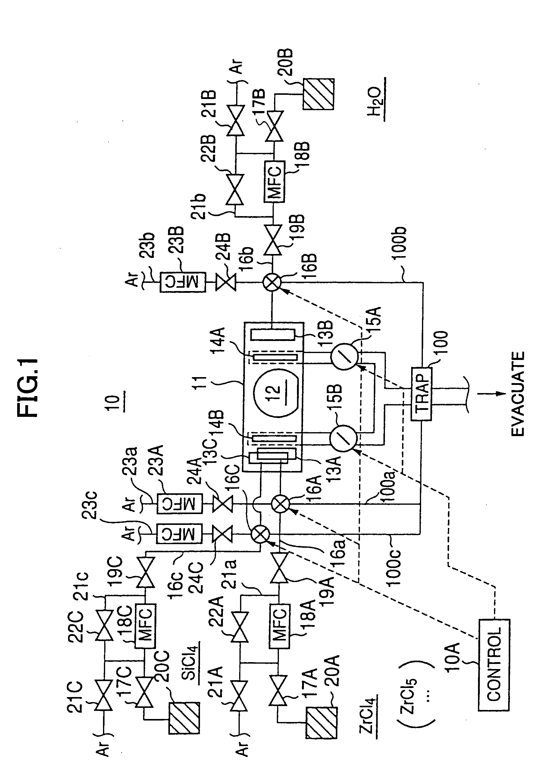
[0170] Referring to FIG. 7, the conductance valves 15A and 15B used with the substrate processing apparatus 10 explained with reference to FIG. 1 through 3 are taken away in the present embodiment, and high-speed rotary valves 25A and 25B are provided in place thereof in an evacuation groove 201a or 201b adjacent to the evacuation openings 14A and 14B. Further, the high-speed rotary valves 25A and 25B are connected to the trap 100 via conduits 207a and 207b respectively.

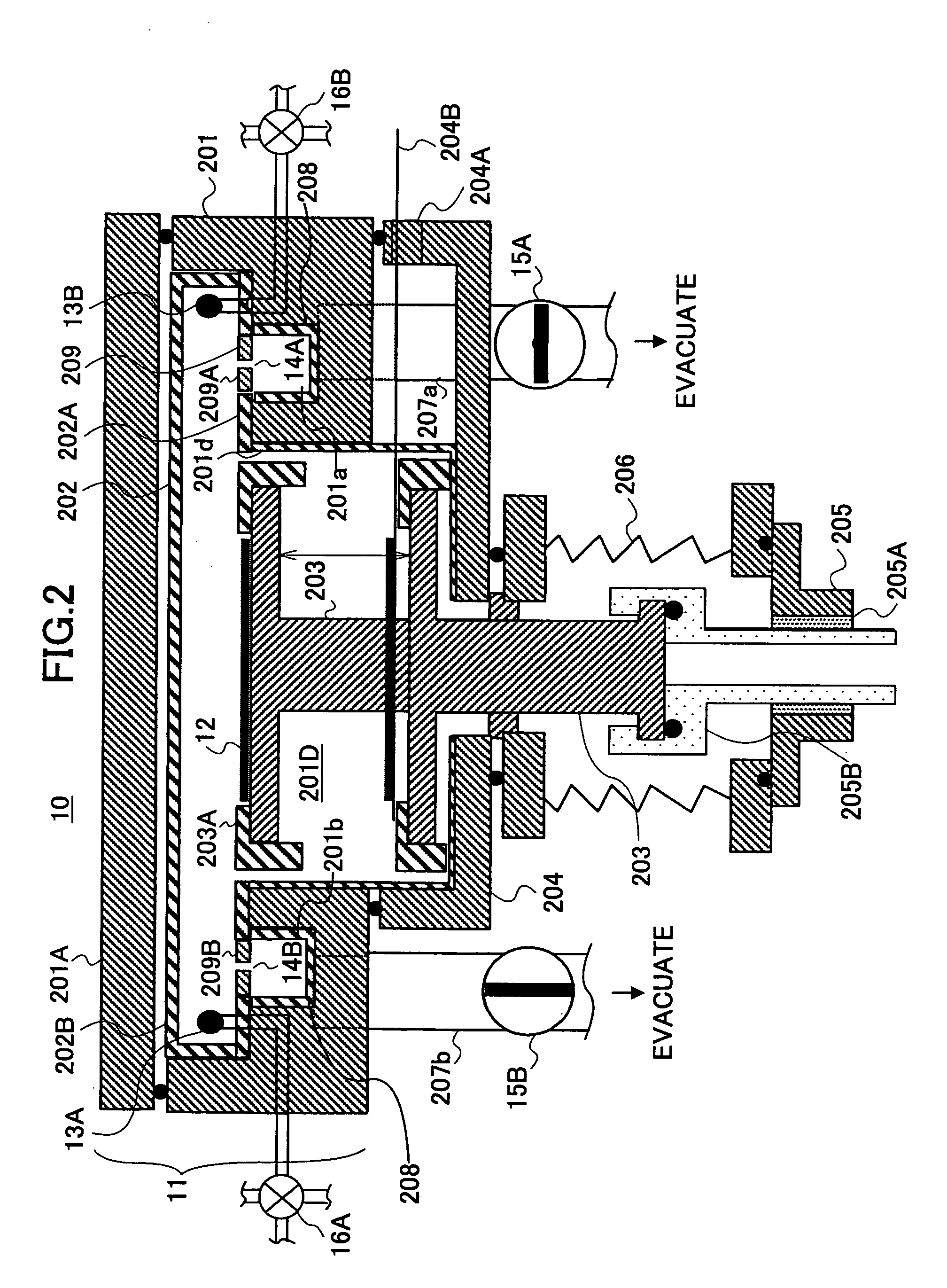
[0171]FIG. 8 shows the construction of the processing vessel 11 in the state that the quartz bottom plate 202A of FIG. 3 is taken away.

[0172] Referring to FIG. 8, there is formed a space in an o...

second embodiment

[0187] [Second Embodiment]

[0188]FIG. 13 shows the construction of a second embodiment of the present invention that forms an Al2O3 film, for example, on the surface of the substrate 12 to be processed by an ALD process by using the substrate processing apparatus 40 of FIG. 7. In FIG. 13, those parts explained previously are provided with the same reference numerals and the explanation thereof will be omitted.

[0189] Referring to FIG. 13, TMA (trimethyl aluminum), for example, is held in the present embodiment in the source material vessel 20A, and the TMA source in the source material vessel 20A is introduced into the quartz reaction vessel 202 in the processing vessel 11 through the switching valve 16A and the nozzle 13A. In the system of FIG. 13, it should be noted that the source supply system including the source material vessel 20C is not used, and thus, the illustration thereof is omitted.

[0190]FIG. 14 is flowchart showing the ALD process carried out by using the system of FI...

third embodiment

[0199] [Third Embodiment]

[0200]FIG. 16 shows the construction of substrate processing apparatus 50 according to a third embodiment of the present invention, wherein those parts of FIG. 16 explained previously are designated with the same reference numerals and the description thereof will be omitted.

[0201] Referring to FIG. 16, the high-speed rotary valve 25B at one side is taken away in the present embodiment, and associated with this, the source gas supply nozzle 13B and also the source gas supply system corresponding thereto are taken away.

[0202] In the substrate processing apparatus 50 of such construction, too, the interior of the quartz reaction vessel 202 is purged at high speed, by fully opening the high-speed rotary valve 25A in the step 21 (chamber purge step) and supplying the Ar gas from the nozzle 13A as shown in the flowchart of FIG. 17. Thus, in the step 22 (oxidizing gas supplying and adsorbing step), the high-speed rotary valve 25A is set to the degree of valve op...


PUM

PropertyMeasurementUnit
Heightaaaaaaaaaa
Heightaaaaaaaaaa
Temperatureaaaaaaaaaa

Abstract

A substrate processing apparatus includes a processing vessel provided with a stage holding thereon a substrate to be processed and evacuated at an evacuation port, and a source gas supplying system that supplies plural source gases to the processing vessel separately in the form of a laminar flow, wherein the evacuation port has a slit-form shape extending in a direction generally intersecting perpendicularly to a direction of the laminar flow, the evacuation port is engaged with a valve having a valve body formed with a slit-form opening corresponding to the slit-form shape of the evacuation port, the slit-form opening being provided so as to cause a displacement with respect to the evacuation port in a direction generally intersecting perpendicularly to an extending direction of the evacuation port, the valve changing a degree of valve opening thereof via displacement of said slit-form opening.

Description

CROSS-REFERENCE TO RELATED APPLICATIONS [0001] The present invention is a continuation-in-part application of PCT / JP03 / 03655 field on Mar. 25, 2003 based on Japanese priority application 2002-086774 and Japanese non-priority basic application 2003-79501 respectively filed on Mar. 26, 2002 and Mar. 24, 2003, the entire contents of each are incorporated by reference. BACKGROUND OF THE INVENTION [0002] The present invention relates to semiconductor devices and particularly to a substrate processing apparatus and a substrate processing method used for production of ultrafine high-speed semiconductor devices having a high-K dielectric film. [0003] With the progress of miniaturization process, a gate length of 0.1 μm or less is becoming possible in ultra high-speed semiconductor devices of these days. Generally, the operational speed of a semiconductor device increases with miniaturization thereof, while there is a need, in such highly miniaturized semiconductor devices, of decreasing the...

Claims


Application Information

Patent Timeline
IPC IPC(8): H01L21/31B08B7/00C23C16/44C23C16/455F16K5/04F16K51/02H01L21/316
CPCB08B7/0035C23C16/4405C23C16/4412C23C16/45504H01L21/31691C23C16/45548F16K5/0407F16K5/0414F16K51/02C23C16/45536H01L21/0228H01L21/02277
Inventor SHINRIKI, HIROSHIARAMI, JUNICHI
Owner TOKYO ELECTRON LTD
Why Eureka
Try Eureka