Low-power direct digital synthesizer with analog interpolation

Active Publication Date: 2005-04-14
QUALCOMM INC
View PDF11 Cites 16 Cited by
  • Summary
  • Abstract
  • Description
  • Claims
  • Application Information

AI Technical Summary

Benefits of technology

An MN counter with analog interpolation (referred to herein as an “MNA counter”) capable of generating an output clock signal having improved jitter performan

Problems solved by technology

This design places stringent requirements on the PLL in terms of performance and power consumption.
This design is undesirable because multiple PLLs for multiple clock signals normally consume a large amount of power and occupy a large area.
In any case, most o

Method used


Image

  • Low-power direct digital synthesizer with analog interpolation
  • Low-power direct digital synthesizer with analog interpolation
  • Low-power direct digital synthesizer with analog interpolation

Examples


Embodiment Construction

The word “exemplary” is used herein to mean “serving as an example, instance, or illustration.” Any embodiment or design described herein as “exemplary” is not necessarily to be construed as preferred or advantageous over other embodiments or designs.

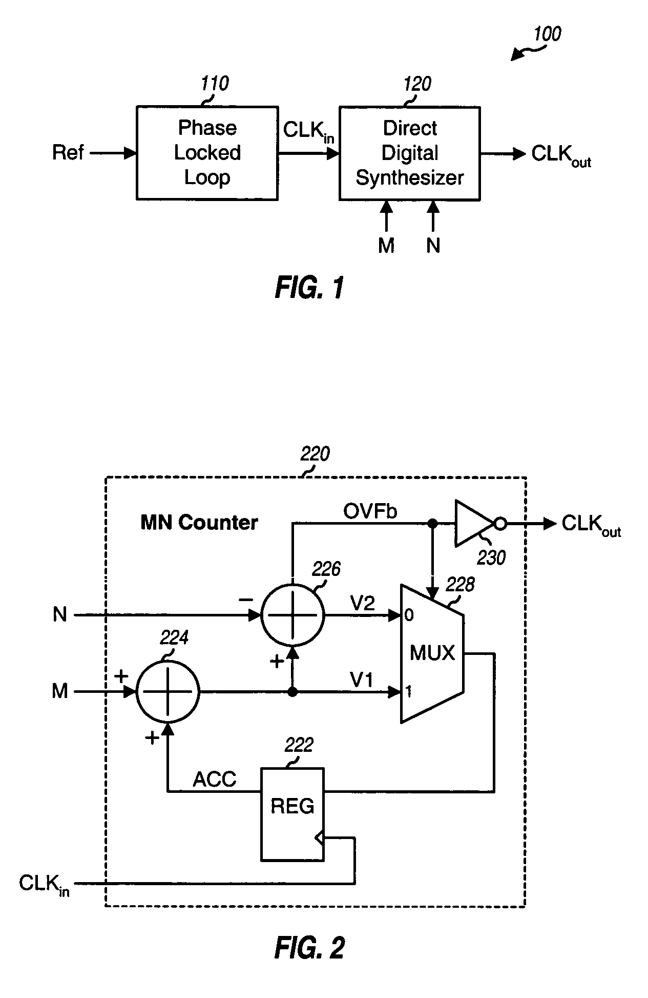
FIG. 1 shows a block diagram of a clock generation subsystem 100 that includes a phase locked loop (PLL) 110 and a direct digital synthesizer (DDS) 120. PLL 110 receives a reference signal (Ref) and generates an input clock signal (CLKin). The input clock signal has its frequency and / or phase locked to that of the reference signal. PLL 110 may be implemented with a phase-frequency detector (PFD), a loop filter, a voltage controlled oscillator (VCO), and a divider, as is known by one skilled in the art. DDS 120 receives the input clock signal and generates an output clock signal (CLKout) having a frequency that is a fraction of the input clock frequency.

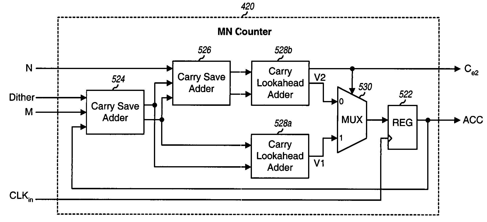
FIG. 2 shows a block diagram of a conventional MN counter 220 that may be used for...


PUM


Abstract

An MN counter with analog interpolation (an “MNA counter”) includes an MN counter, a multiplier, a delay generator, and a current generator. The MN counter receives an input clock signal and M and N values, accumulates M for each input clock cycle using a modulo-N accumulator, and provides an accumulator value and a counter signal with the desired frequency. The multiplier multiplies the accumulator value with an inverse of M and provides an L-bit control signal. The current generator implements a current locked loop that provides a reference current for the delay generator. The delay generator is implemented with a differential design, receives the counter signal and the L-bit control signal, compares a differential signal generated based on the counter and control signals, and provides the output clock signal. The leading edges of the output clock signal have variable delay determined by the L-bit control signal and the reference current.

Description

BACKGROUND I. Field The present invention relates generally to electronics circuits, and more specifically to a direct digital synthesizer (DDS). II. Background In a modem communication device, multiple clock signals with frequencies that are unrelated may be needed for various functions. For example, a clock signal with a first frequency may be needed for a digital signal processing subsystem, another clock signal with a second frequency may be needed for a sampled analog subsystem, and so on. Multiple clock signals with unrelated frequencies may be generated in various manners. In one conventional design, a clock generator with a single phase locked loop (PLL) is operated at a high frequency. The clock signal from this generator is divided in frequency by different integer values to obtain multiple output clock signals with different frequencies. This design places stringent requirements on the PLL in terms of performance and power consumption. In another conventional design,...

Claims


Application Information

Patent Timeline
IPC IPC(8): G06F1/02G06F1/08H03K3/017H03K5/00H03K5/135H03K5/156H03K23/68H03L7/081
CPCG06F1/022G06F1/08G06F2211/902H03L7/0814H03K5/1565H03K2005/00032H03K2005/00071H03K5/135H03L7/0816G06F1/02H03K3/00H03K5/13
Inventor FAHIM, AMR M.
Owner QUALCOMM INC
Why Eureka
Try Eureka