High-frequency circuit

a high-frequency circuit and circuit technology, applied in the direction of transformer/inductance details, coils, resonators, etc., can solve the problems of high cost, unrealistic improvement of strip formation precision, and inability to meet the requirements of high-frequency circuits, so as to reduce resonance frequency, broad-band filter characteristics, and energy transmission efficiency

Active Publication Date: 2005-04-14
PANASONIC CORP
View PDF4 Cites 36 Cited by
  • Summary
  • Abstract
  • Description
  • Claims
  • Application Information

AI Technical Summary

Benefits of technology

[0037] In order to obtain a strong coupling between an external circuit and the stacked spiral conductive strip resonator, it is preferable to obtain a coupling by directly connecting a portion of the spiral conductive strip to a portion of the input / output line.
[0038] As a result, not only the efficiency of energy transmission from an external circuit to the stacked spiral conductive strip resonator, or from the stacked spiral conductive strip resonator to an external circuit can be improved, but also broad-band filter characteristics can be obtained.
[0039] Preferably, if the first and second spiral conductive strips were to be placed on each other so that a spiral center of each spiral conductive strip coincides, outer peripheries of the first and second spiral conductive strips would coincide with each other.
[0040] As a result, the capacitance which couples the first spiral conductive strip and the second spiral conductive strip increases at an overlapping portion between the first spiral conductive strip and the second spiral conductive strip. Therefore, a current transfer via an overlapping coupling capacitance between the spiral conductive strips can occur at an even lower frequency. As a result, a further reduction in the resonance frequency becomes possible, i.e., a more compact resonator can be provided.
[0041] More preferably, an open terminating end of an outermost strip subportion of the first spiral conductive strip and an open terminating end of an outermost strip subportion of the second spiral conductive strip are disposed diagonally opposite from each other with respect to the spiral center of the first spiral conductive strip.
[0042] Thus, an effective overlapping between the spiral conductive strips can be realized in the outermost strip subportion, which has the longest distance per turn around the spiral center of the spiral conductive strip. Therefore, a current transfer via an overlapping coupling capacitance between the spiral conductive strips can occur at an even lower frequency. As a result, a further reduction in the resonance frequency becomes possible, i.e., a more compact resonator can be provided.

Problems solved by technology

However, substrate materials having high dielectric constant are more expensive than substrate materials having low dielectric constant, e.g., resin.
Therefore, the aforementioned technique of downsizing a resonator by using a material with high dielectric constant for the circuit substrate leads to cost problems, regardless of whether the entire circuit is formed by using a substrate of a material with high dielectric constant or only the resonator portion is formed of a material with high dielectric constant.
However, given the current demands for reducing costs associated with production processes, it is not realistic to improve strip formation precision just for the sake of realizing an extreme reduction in the distance between parallel lines of a resonator.
Thus, it would be unrealistic to provide a resonator having a short resonator length by reducing the distance between parallel coupled-lines.
However, the technique illustrating FIG. 27, where two transmission lines are disposed in multiple layers so as to overlap each other in the thickness direction has the following two problems.
A first problem is that there is a limit to the reduction in resonance frequencies that can be achieved based on the capacitance obtained by the parallel overlapping of the two transmission lines 904 and 905.
This technique is only effective for causing a resonance in the case where the length of the coupled-lines is ½ of the wavelength of the electromagnetic waves.
Thus, the length of the coupled-lines is still required to be about ½ of the wavelength, which is a limitation to downsizing.
A second problem is that the resonance obtained from parallel coupled-lines cannot provide adequate spurious prevention characteristics.
A resonator which is based on parallel coupled-lines is not entirely suitable for use in a communications module since it is impossible to control a resonance which occurs at a frequency which is twice the fundamental frequency.

Method used


Image

  • High-frequency circuit
  • High-frequency circuit
  • High-frequency circuit

Examples


first embodiment

[0105] (First Embodiment)

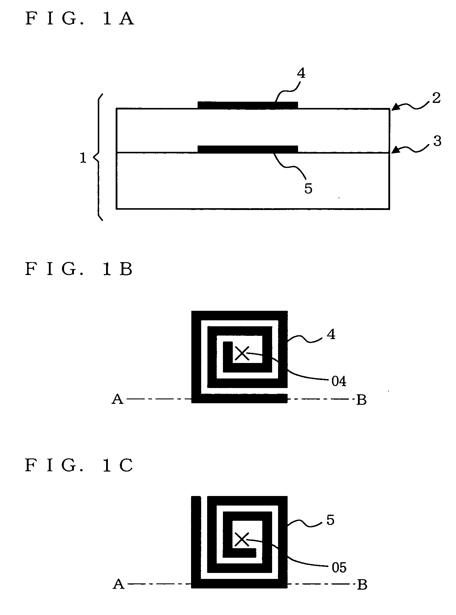
[0106]FIG. 1A is a schematic cross-sectional view showing a high-frequency circuit according to a first embodiment of the present invention taken along line AB in FIGS. 1B and 1C. The high-frequency circuit according to the present embodiment is formed on a multilayered dielectric substrate 1 which has two conductive circuit layers. FIG. 1B is an upper plan view showing a pattern of a spiral conductive strip 4 which is formed on an outermost surface 2 of an upper conductive circuit layer in the multilayered dielectric substrate 1. FIG. 1C is an upper plan view showing a pattern of a spiral conductive strip 5 formed on an interface 3 of a lower conductive circuit layer in the multilayered dielectric substrate 1.

[0107] In the high-frequency circuit according to the first embodiment, the spiral conductive strip 4 is formed on the surface of an uppermost conductive circuit layer in the multilayered dielectric substrate 1 and the spiral conductive strip 5 is for...

second embodiment

[0123] (Second Embodiment)

[0124]FIG. 9A is a schematic cross-sectional view showing a high-frequency circuit according to a second embodiment of the present invention taken along line CD in FIGS. 9B, 9C, and 9D. The high-frequency circuit according to the present invention is formed on a multilayered dielectric substrate 1 which has three dielectric circuit layers. FIG. 9B is an upper plan view showing a pattern of a spiral conductive strip 4 which is formed on an outermost surface 2 of an uppermost conductive circuit layer in the multilayered dielectric substrate 1. FIG. 9C is an upper plan view showing a pattern of a spiral conductive strip 5 formed on an interface 3 of an intermediate conductive circuit layer in the multilayered dielectric substrate 1. FIG. 9D is an upper plan view showing a pattern of a spiral conductive strip 9 formed on an interface 8 of a lowermost conductive circuit layer in the multilayered dielectric substrate 1.

[0125] If the outermost surface 2, the inte...

third embodiment

[0132] (Third Embodiment)

[0133]FIG. 10A is a schematic cross-sectional view showing a high-frequency circuit according to a third embodiment of the present invention taken along line EF in FIGS. 10B and 10C. The high-frequency circuit according to the third embodiment is formed on a multilayered dielectric substrate 1 which has two dielectric circuit layers. FIG. 10B is an upper plan view showing patterns of a spiral conductive strip 4 and an input / output line 12 which are formed on an outermost surface 2 of an upper conductive circuit layer in the multilayered dielectric substrate 1. FIG. 10C is an upper plan view showing a pattern of a spiral conductive strip 5 formed on an interface 3 of a lower conductive circuit layer in the multilayered dielectric substrate 1.

[0134] As in the case of the first embodiment, point 04 shown in FIG. 10B and point O5 shown in FIG. 10C are in identical positions within each plane. The layered spiral conductive strips 4 and 5 together compose a stack...


PUM

PropertyMeasurementUnit
resonance frequencyaaaaaaaaaa
lengthaaaaaaaaaa
dielectric constantaaaaaaaaaa

Abstract

A high-frequency circuit is formed on a multilayered dielectric substrate 1 having at least two conductive circuit layers. The high-frequency circuit includes: a first spiral conductive strip 4 formed in the first conductive circuit layer, the first spiral conductive strip having at least one turn; and a second spiral conductive strip 5 formed in a second conductive circuit layer which is different from the first conductive circuit layer, the second spiral conductive strip having at least one turn and not being in electrical conduction with the first spiral conductive strip. The first spiral conductive strip and the second spiral conductive strip, located at different levels, overlap each other. The first spiral conductive strip has a rotating direction opposite to a rotating direction of the second spiral conductive strip.

Description

[0001] This application is a continuation of International Application PCT / JP2004 / 004759, filed Apr. 1, 2004.BACKGROUND OF THE INVENTION [0002] 1. Field of the Invention [0003] The present invention relates to a high-frequency circuit which is capable of transmitting or radiating a high-frequency signal in the microwave or millimeter range, and more particularly to a high-frequency circuit capable of exhibiting resonance. [0004] 2. Description of the Background Art [0005] In recent years, wireless communication devices have made advancements in terms of downsizing and high-functionalization, which have enabled the drastic prevalence of cellular phones. In the years to come, further downsizing, high-functionalization, and cost reduction are expected. [0006] A high-frequency circuit which is mounted in a wireless communication device such as a cellular phone requires a resonator as an element for composing circuits such as filters, an antenna, and the like. [0007] For example, a ½ wav...

Claims


Application Information

Patent Timeline
Patent Type & Authority Applications(United States)
IPC IPC(8): H01P1/203H01P5/18H01P7/08
CPCH01P1/20381H01P5/185H01P7/084H01P7/082H01P5/187
Inventor KANNO, HIROSHISAKIYAMA, KAZUYUKISANGAWA, USHIOFUJISHIMA, TOMOYASU
Owner PANASONIC CORP
Why Eureka
Try Eureka