

Superconducting circuit
a superconducting latch and driver technology, applied in the direction of code conversion, instruments, pulse techniques, etc., can solve the problems of reducing the operating margin of the sfq circuit, and it is difficult to drive signal lines with large characteristic impedance directly at high speed, so as to reduce ground ripples and facilitate output a plurality
- Summary
- Abstract
- Description
- Claims
- Application Information
AI Technical Summary
Benefits of technology
Problems solved by technology
Method used
Image

Examples
second embodiment
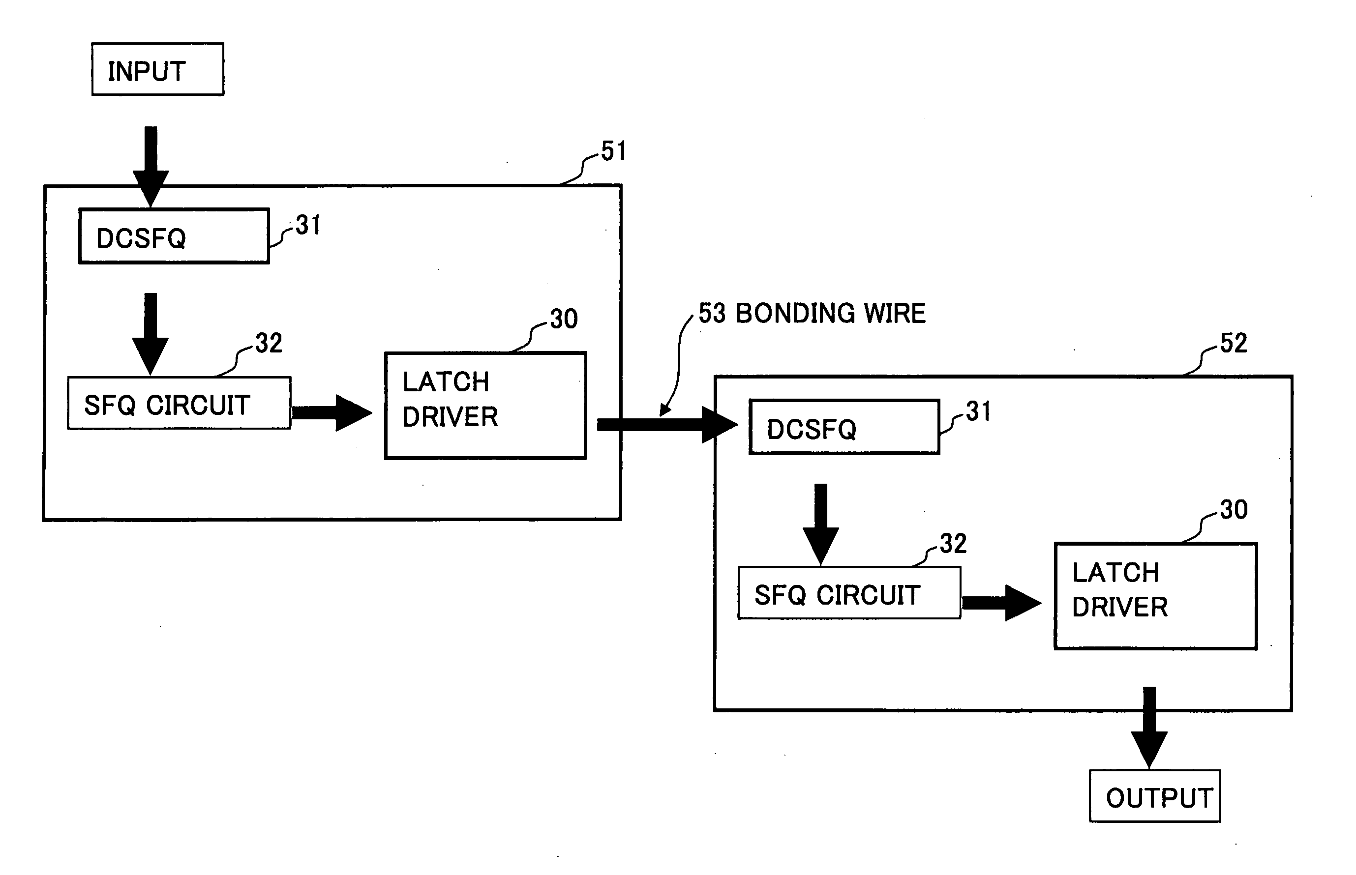
FIG. 14 is an illustrative drawing showing the superconducting SFQ circuit according to the second aspect of the invention. In FIG. 14, the same elements as those of FIG. 13 are referred to by the same numbers, and a description thereof will be omitted.
In FIG. 14, a chip 110B, which is a superconducting SFQ circuit according to the invention, includes the superconducting circuit 111A, the superconducting circuit 112A, and the n stages of superconducting SFQ circuits 113A-1 through 113A-n. The superconducting SFQ circuits 113A-1 through 113A-n make up a Josephson transmission line (JTL) The superconducting SFQ circuit 113A-x (x=1, 2, . . . , n) includes the ground plane 115-x, the inductance 116-x, the Josephson junction 117-x, the Josephson junction 118-x, and the inductances LUx and LLx that provide connections with adjoining circuits.
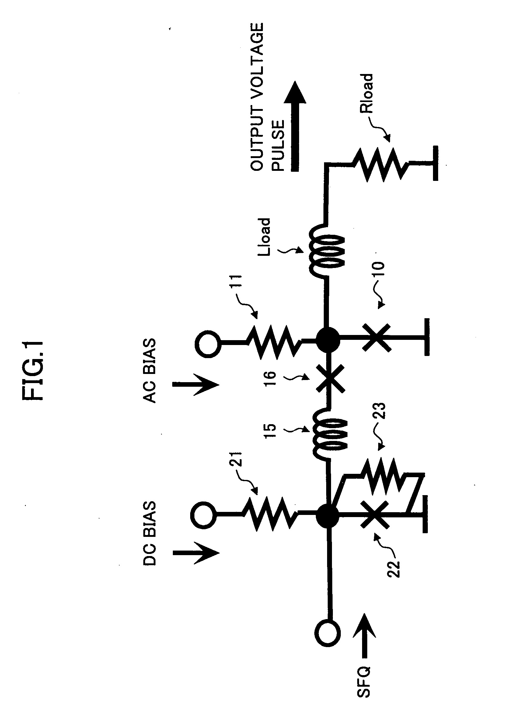
The higher the frequency, the greater the impedance of inductance becomes. Even if the ground potential of the superconducting circuit 112A fluctu...
third embodiment
FIG. 15 is an illustrative drawing showing the superconducting SFQ circuit according to the second aspect of the invention. In FIG. 15, the same elements as those of FIG. 14 are referred to by the same numbers, and a description thereof will be omitted.
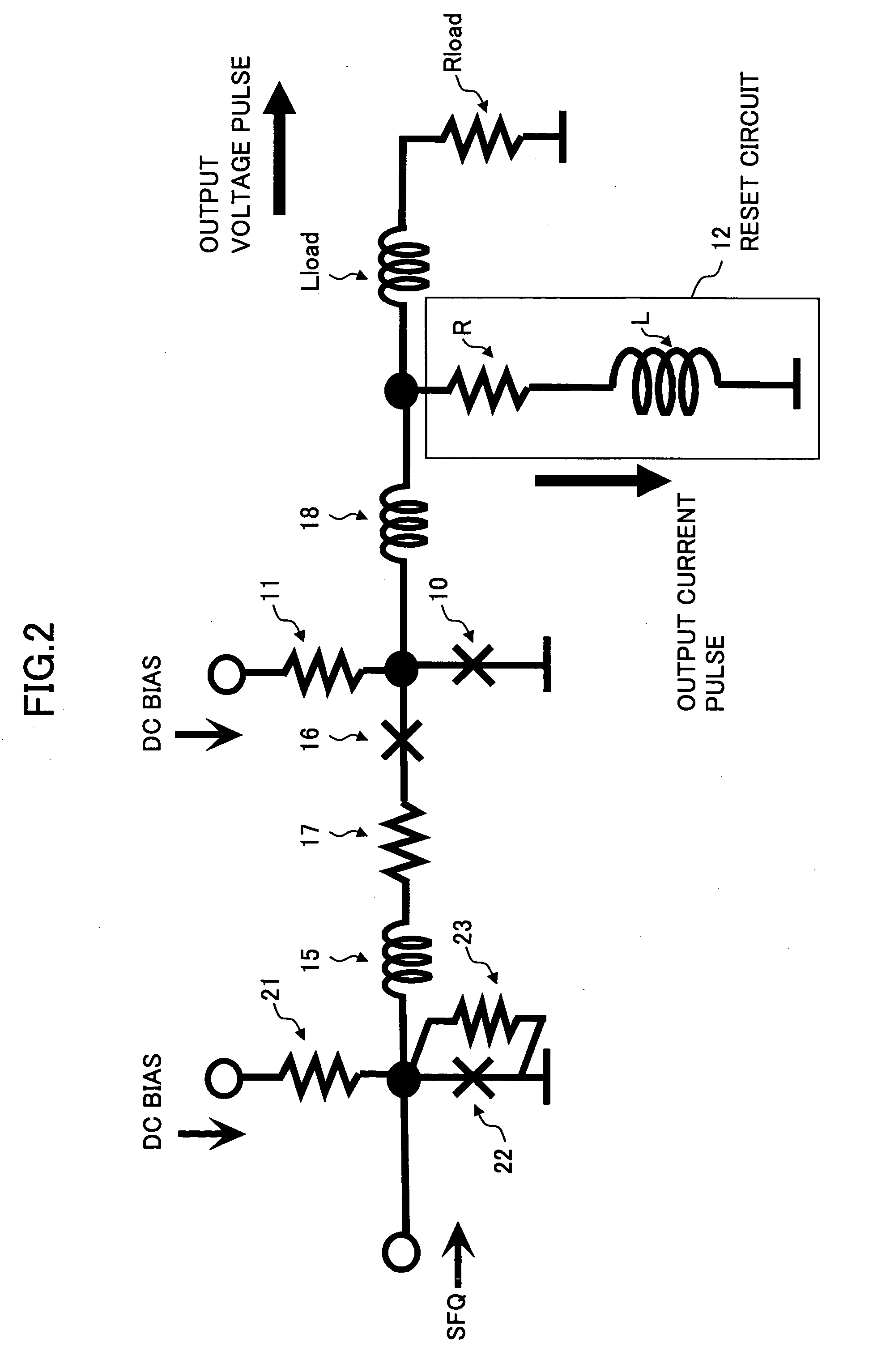
In FIG. 15, a chip 110C, which is a superconducting SFQ circuit according to the invention, includes the superconducting circuit 111A, a superconducting circuit 112C, and the n stages of superconducting SFQ circuits 113A-1 through 113A-n. The superconducting SFQ circuits 113A-1 through 113A-n make up a Josephson transmission line. The superconducting SFQ circuit 113A-x (x=1, 2, . . . , n) includes the ground plane 115-x, the inductance 116-x, the Josephson junction 117-x, the Josephson junction 118-x, and the inductances LUx and LLx that provide connections with adjoining circuits. A resistance Rx is provided on the DC+ side and a resistance RGx is provided on the DC− side of the superconducting SFQ circuit 113A-x. Such resistance is...
fourth embodiment
FIG. 16 is an illustrative drawing showing the superconducting SFQ circuit according to the second aspect of the invention. In FIG. 16, the same elements as those of FIG. 12 are referred to by the same numbers, and a description thereof will be omitted.
The construction shown in FIG. 16 is characterized in that a plurality of superconducting circuits 111 are provided in a single chip 110D, and are coupled via the separation-purpose (isolation-purpose) superconducting SFQ circuits 113-1 through 113-n. Further, the superconducting circuit 112 such as an output circuit driven by an AC bias is coupled to the adjacent superconducting circuit 111 through the superconducting SFQ circuits 113-1 through 113-n in the same manner as in the construction shown in FIG. 12.
Even if two or more superconducting circuits are connected to each other as shown in FIG. 16, the provision of the separation-purpose superconducting SFQ circuits between superconducting circuits makes it possible to suppress ...
PUM
 Abstract
Description
Claims
Application Information