Process monitoring using infrared optical diagnostics

a technology of infrared optical diagnostics and process monitoring, applied in the direction of optical radiation measurement, instruments, vacuum evaporation coating, etc., can solve the problems of inability to use non-plasma processes such as film deposition, inefficient, and time-consuming post-process analysis methods, etc., to achieve the effect of improving the process

Inactive Publication Date: 2005-04-21
TOKYO ELECTRON LTD
View PDF10 Cites 39 Cited by
  • Summary
  • Abstract
  • Description
  • Claims
  • Application Information

AI Technical Summary

Benefits of technology

[0014] It is a further object of the present invention to correlate resulting gaseous environments in the process chamber with physical properties of the processed wafers and to improve the process by optimizing process conditions and detecting trends of departure from target values.

Problems solved by technology

This method of post-process analysis is time consuming, inefficient, and becomes increasingly more expensive as the wafer size increases.
However, it cannot be used in non-plasma processes such as film deposition, and the optical emission spectrum from plasma processes can be very complicated.
Furthermore, OES does not provide direct information about the substrate during a process step.
The aforementioned disadvantages using post-process analysis show that there is a need for non-invasive methods for monitoring of semiconductor processes that allow for comprehensive analysis of the gaseous environment and the substrate during a process step.

Method used


Image

  • Process monitoring using infrared optical diagnostics
  • Process monitoring using infrared optical diagnostics
  • Process monitoring using infrared optical diagnostics

Examples


Embodiment Construction

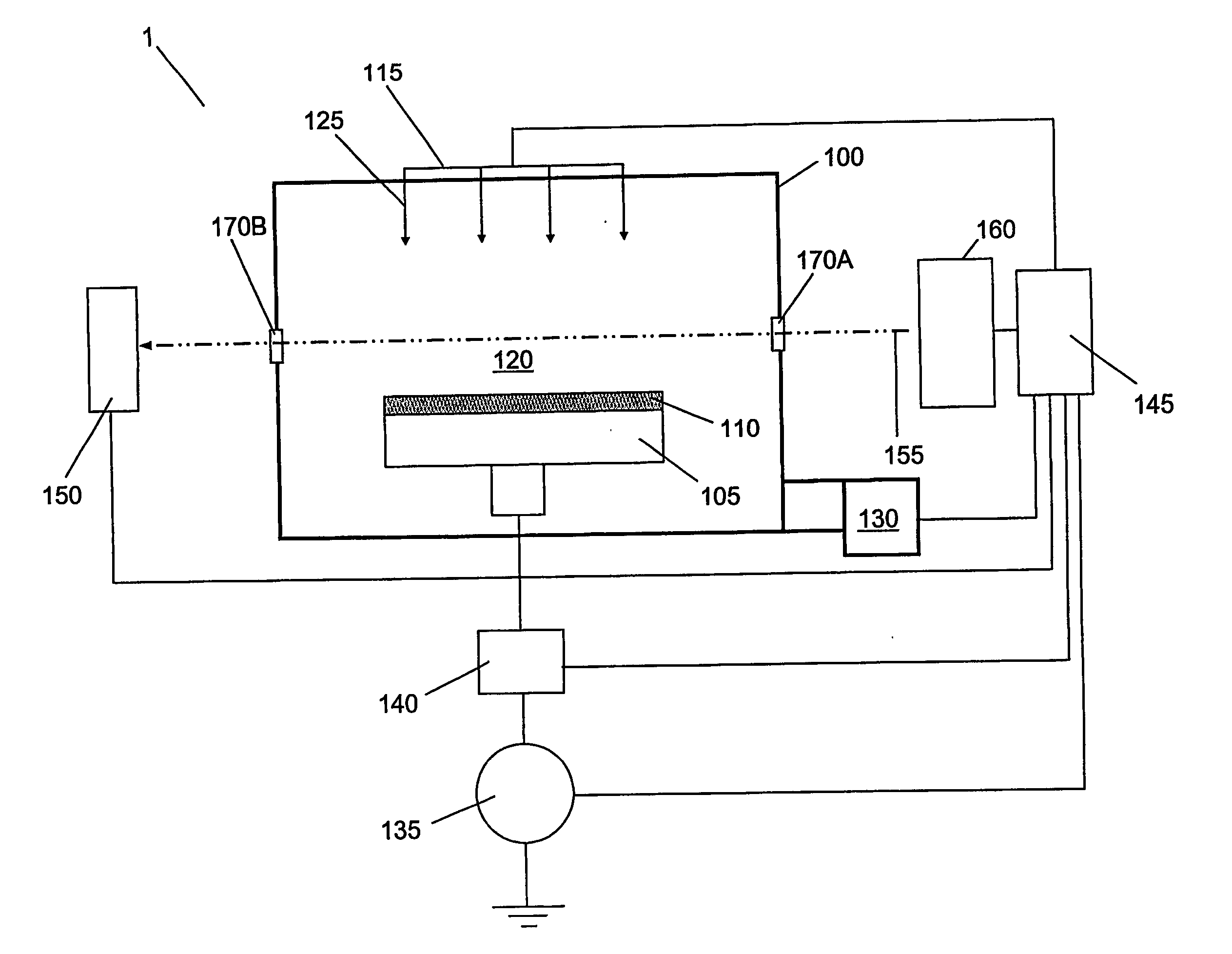
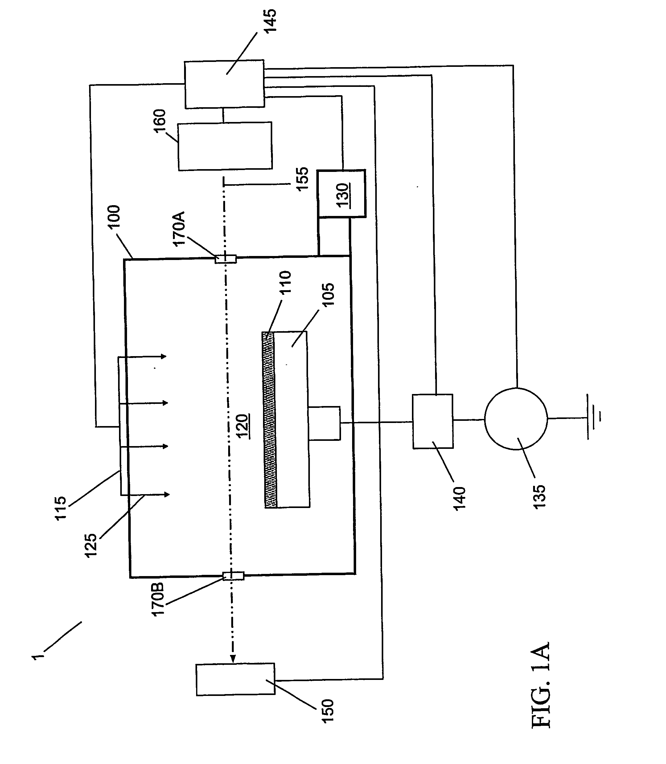
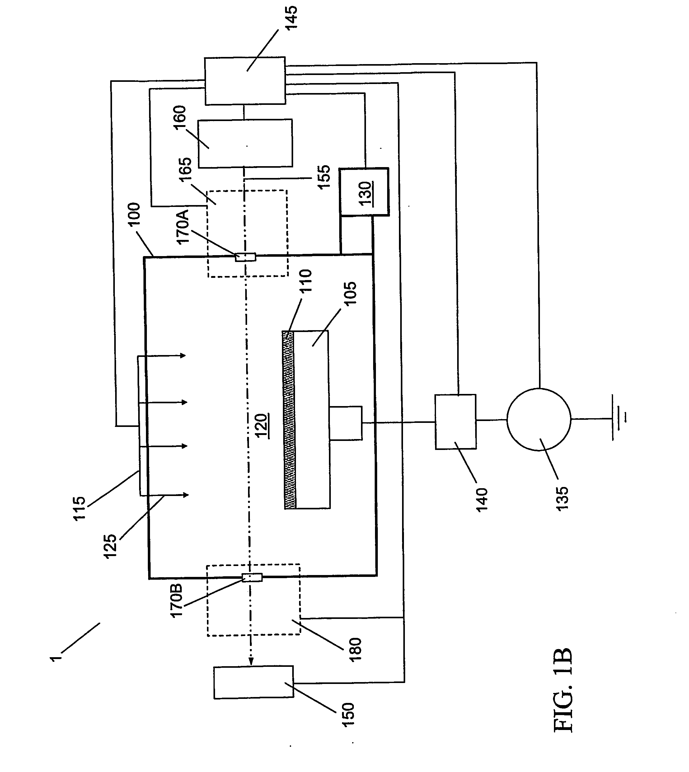
[0023] In general, the present invention provides an apparatus and a method for carrying out real-time in-situ process monitoring during a semiconductor process using infrared spectroscopy. The process can comprise deposition or etching steps that are carried out in the presence of a plasma or by thermal reactions in the absence of a plasma. In the Figures, like reference numbers are used to indicate like elements throughout.

[0024] One aspect of the current invention is detecting and monitoring the gaseous environment in the processing system during etching or deposition steps. This is carried out using FT-ITAS to identify and monitor gaseous species of interest in the processing system and detecting trends of departure from target values. Another aspect of the current invention is applying FT-ITAS to chamber cleaning and chamber conditioning. Yet another aspect of the current invention is using FT-RAIRS for identifying and monitoring chemical species adsorbed on a substrate during...


PUM

PropertyMeasurementUnit
frequencyaaaaaaaaaa
frequencyaaaaaaaaaa
pressuresaaaaaaaaaa

Abstract

A method and apparatus for real-time monitoring of the substrate and the gaseous process environment in a semi-conductor process step is described. The method uses infrared spectroscopy for in-situ analysis of gaseous molecular species in the process region and characterization of adsorbed chemical species on a substrate. The process monitoring can be applied to endpoint-and fault detection in etching and deposition processes, in addition to chamber cleaning and chamber condition steps.

Description

CROSS-REFERENCE TO RELATED APPLICATIONS [0001] This application claims priority and is related to U.S. Application Ser. No. 60 / 365,529, filed on Mar. 20, 2002. This application is related to U.S. Application Ser. No. 60 / 352,546, filed Jan. 31, 2002 and Ser. No. 10 / 096,932, filed Mar. 14, 2002. The contents of all of these applications are incorporated herein by reference in their entirety.BACKGROUND OF THE INVENTION [0002] 1. Field of the Invention [0003] The present invention relates to real-time in-situ monitoring of semiconductor processing. The invention uses infrared spectroscopy to monitor the substrate and the gaseous environment during a process. [0004] 2. Background of the Invention [0005] Advanced process control that involves in-situ process monitoring and fault detection in semiconductor manufacturing is essential for reproducible production of complex structures. Introduction of new materials and smaller dimensions into integrated circuits results in the need for improv...

Claims


Application Information

Patent Timeline
Patent Type & Authority Applications(United States)
IPC IPC(8): C23C14/54C23C16/52G01J5/02G01N21/35
CPCC23C14/54H01J37/32972G01N21/3504C23C16/52
Inventor LUDVIKSSON, AUDUNN
Owner TOKYO ELECTRON LTD
Why Eureka
Try Eureka