Group iii nitride semiconductor device and its method of manufacture

a nitride semiconductor and semiconductor technology, applied in the direction of sustainable manufacturing/processing, polycrystalline material growth, final product manufacturing, etc., can solve the problems of a sic wafer dimensioned to 1 cm1 cm, a 3.5% mismatch between the lattice constant of gan and sic, and a cost of 200 us dollars. to achieve the effect of reducing stress

Active Publication Date: 2005-04-21
EPISTAR CORP
View PDF2 Cites 11 Cited by
  • Summary
  • Abstract
  • Description
  • Claims
  • Application Information

AI Technical Summary

Benefits of technology

[0014] It is another objective of this invention to provide a process implementing a stress-absorbing layer located between a silicon substrate and a Group III nitride semiconductor to alleviate stress resulted from different lattice constants between the Group III nitride substance and the silicon substrate, thereby preventing cracking of the Group III nitride semiconductor due to the stress.
[0016] It is yet a further objective of this invention to provide a Group III nitride semiconductor device implementing a stress-absorbing layer located between a silicon substrate and a Group III nitride semiconductor to alleviate stress resulted from different lattice constants between the Group III nitride substance and the silicon substrate, thereby preventing cracking of the Group III nitride semiconductor due to the stress.
[0024] According to one aspect of this invention, the amorphous aluminum nitride pre-layer rearranges with the aluminum interlayer during formation to alleviate stress between the amorphous aluminum nitride pre-layer and the silicon substrate.
[0042] According to one aspect of this invention, the amorphous aluminum nitride pre-layer rearranges with the aluminum interlayer during formation to alleviate stress between the amorphous aluminum nitride pre-layer and the silicon substrate.

Problems solved by technology

First, the cost of a sapphire wafer dimensioned to 2-inch diameter is about 65-240 US dollars, and the cost of a SiC wafer dimensioned to 1 cm×1 cm is about 200 US dollars, both of which are relatively expensive.
Secondly, there is about 3.5% mismatch between the lattice constants of GaN and SiC, and an even greater mismatch between GaN and sapphire, about 16%.
Thirdly, as sapphire being an insulating material, electrodes cannot be deposited on a backside of the sapphire substrate, resulting a more expensive process for forming electrodes in subsequent processes.
Fourthly, the thermal expansion coefficients of sapphire and GaN differ significantly, resulting in more complicated growing processes.
However, because a monocrystalline GaN layer cannot be smoothly deposited on the Si substrate, most GaN takes the form of GaN crystalline pillars in the shape of hexagonal cones.
Secondly, the stress resulted from the different lattice constants between GaN and the silicon substrate would accumulate and cause cracking of the GaN epitaxy layer, as shown in FIG. 6, to cause inability of subsequent manufacturing of devices.

Method used


Image

  • Group iii nitride semiconductor device and its method of manufacture
  • Group iii nitride semiconductor device and its method of manufacture
  • Group iii nitride semiconductor device and its method of manufacture

Examples


Embodiment Construction

)

[0063] A few embodiments according to this invention are described in detail are follows. However, these embodiments are provided for exemplification purposes but not to limited the scope of protection. This invention may also be implemented in many other embodiments. The scope of this invention should be determined by the appended claims.

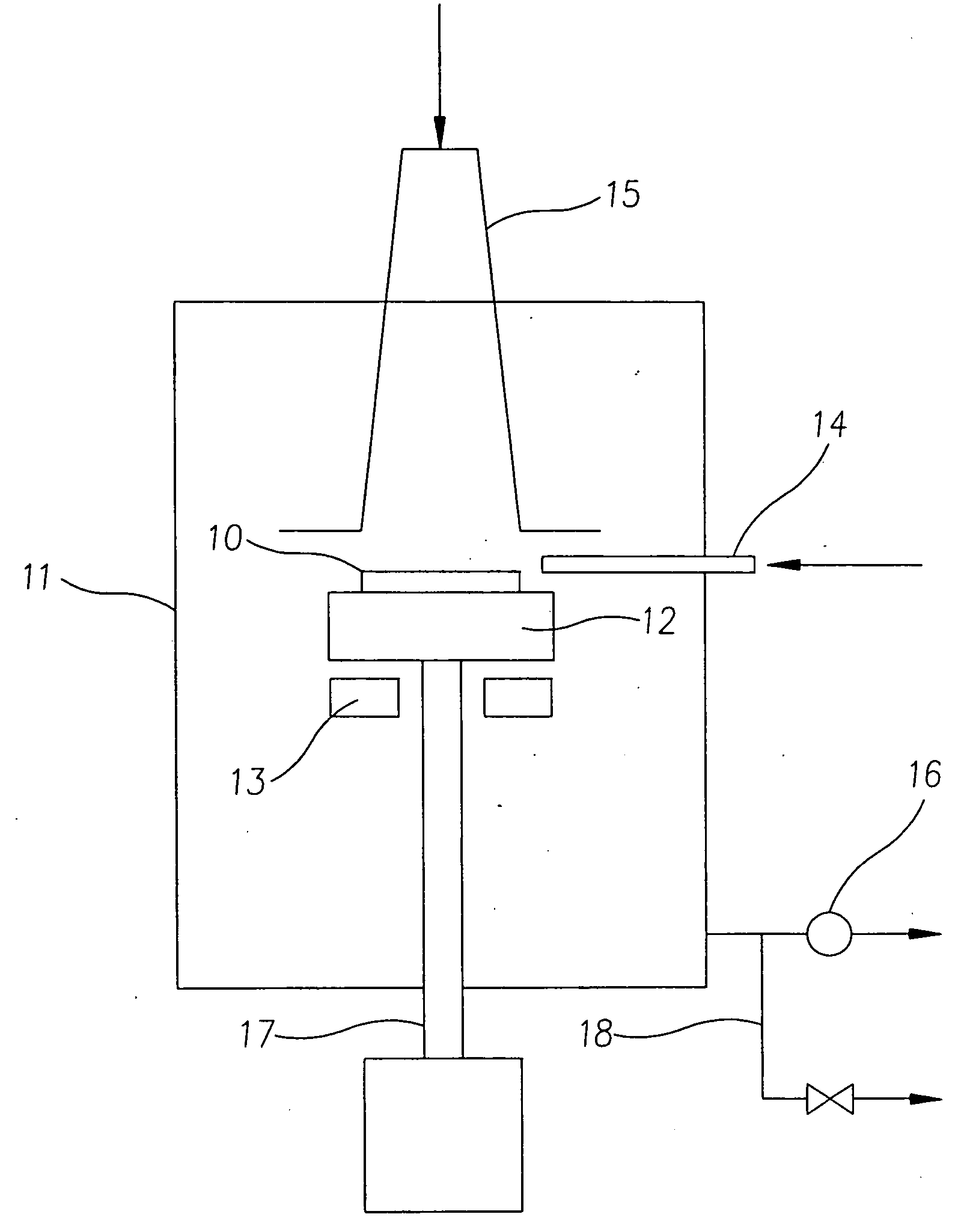
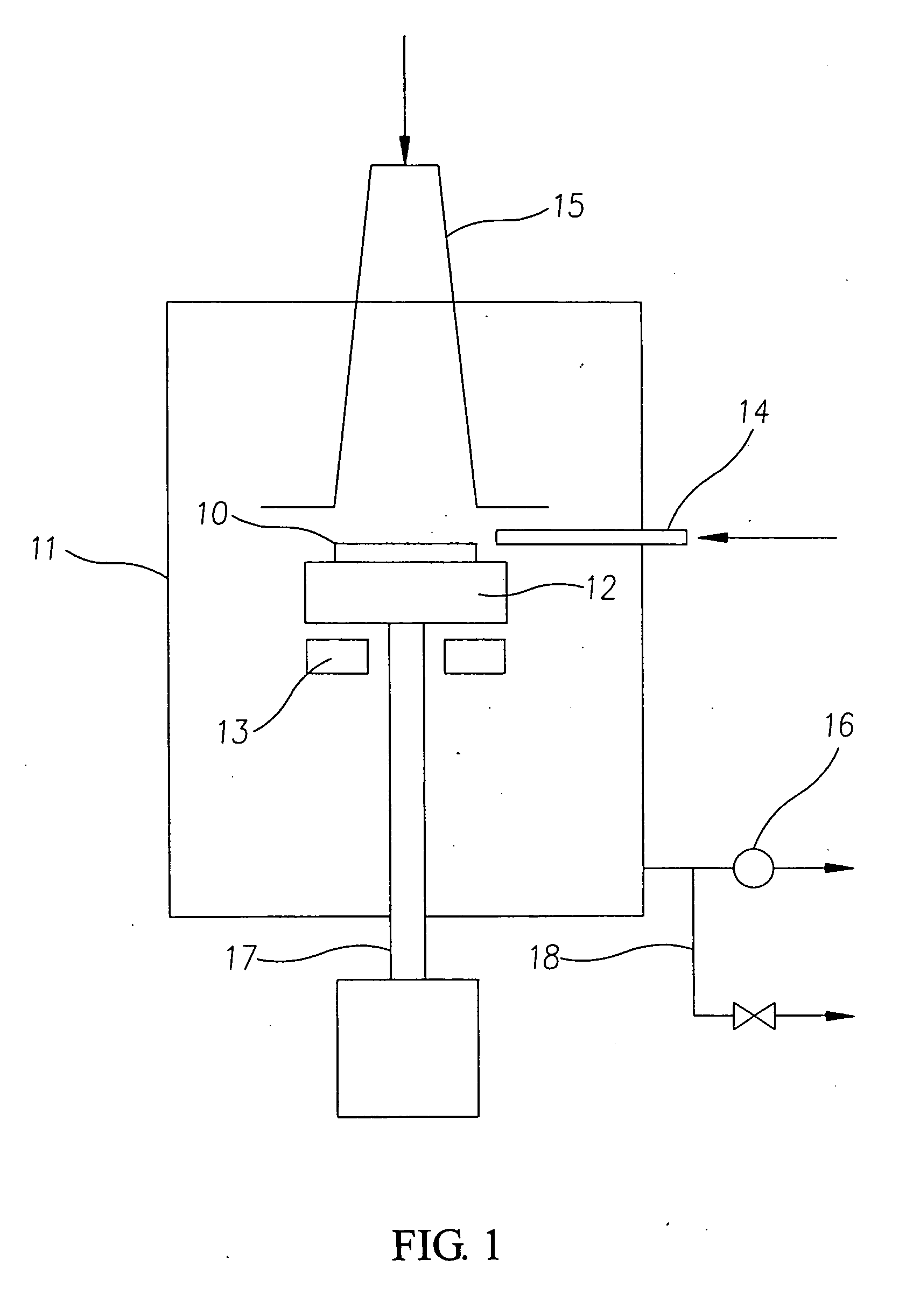
[0064] To overcome the interfacing difficulties existed between the GaN layer and conventional Si substrate, this invention adds a stress-absorbing layer to the above laminar structure consisting of numerous layers of different properties, as shown in FIG. 7, which illustrates a laminar cross-section of a first embodiment of a semiconductor device according this invention. As illustrated, a Si substrate 71 includes a stress-absorbing layer 72 that is constructed of an amorphous silicon nitride layer 721, an aluminum interlayer 722, an amorphous aluminum nitride pre-layer 723 and a polycrystalline Group III nitride layer containing aluminum 724, t...


PUM

PropertyMeasurementUnit
thickaaaaaaaaaa
diameteraaaaaaaaaa
pressureaaaaaaaaaa

Abstract

Disclosed is a Group III nitride semiconductor device comprising a stress-absorbing layer having: an amorphous silicon nitride layer, an aluminum interlayer, an amorphous aluminum nitride pre-layer and a polycrystalline Group III nitride layer containing aluminum. The stress-absorbing layer is located between a silicon substrate and a Group III nitride semiconductor, for alleviating stress resulted from different lattice constants between the Group III nitride substance and the silicon substrate, thereby preventing cracking of the Group III nitride semiconductor due to the stress. Further disclosed is a method of manufacturing Group III nitride semiconductor device.

Description

CROSS-REFERENCES TO RELATED APPLICATIONS [0001] Not Applicable STATEMENT REGARDING FEDERALLY SPONSORED RESEARCH OR DEVELOPMENT [0002] Not Applicable DESCRIPTION [0003] 1. Field of Invention [0004] This invention relates to a Group III nitride semiconductor device and its method of manufacture, particularly to one implementing a stress-absorbing layer located between a silicon substrate and a Group III nitride semiconductor to alleviate stress resulted from different lattice constants between the Group III nitride substance and the silicon substrate, thereby preventing cracking of the Group III nitride semiconductor due to the stress. [0005] 2. Background [0006] The processes for depositing high-quality GaN-based compound film are generally categorized into two types. One implements the metal-organic chemical vapor deposit (MOCVD) process or plasma-enhanced MOCVD process, which is a modification of MOCVD, and is characterized by the use of a representative reactor pressure of 10-1030...

Claims


Application Information

Patent Timeline
Patent Type & Authority Applications(United States)
IPC IPC(8): C30B25/02C30B29/40H01L21/20H01L21/205H01L29/20H01L31/0304H01L31/18H01L33/00H01L33/12H01L33/16
CPCC30B25/02Y02E10/544H01L21/02381H01L21/02458H01L21/02488H01L21/02491H01L21/02505H01L21/02513H01L21/0254H01L29/2003H01L31/03046H01L31/1852H01L33/007H01L33/12H01L33/16C30B29/40Y02P70/50
Inventor TSAI, TZONG-LIANGCHANG, CHIH-SUNG
Owner EPISTAR CORP
Why Eureka
Try Eureka