Method and structure to suppress external latch-up

a technology of latch-up and internal latch-up, which is applied in the direction of semiconductor devices, electrical apparatus, transistors, etc., can solve the problems of premature failure of ic devices, immediate failure of devices, circuits or systems, and devices that are increasingly susceptible to failure, so as to improve the use of chip protection

Inactive Publication Date: 2005-04-21
IBM CORP
View PDF26 Cites 39 Cited by
  • Summary
  • Abstract
  • Description
  • Claims
  • Application Information

AI Technical Summary

Benefits of technology

[0020] Aspects of the present invention feature a method and structure for suppression of latch-up within integrated circuits (ICs). ICs designed in accordance with the present invention contain substrate and well contacts that vary in periodicity, thus distance between adjacent contacts will vary. This disclosure recognizes that injected current density wil

Problems solved by technology

Use of thinner gate oxides, however, results in devices that are increasingly susceptible to failure arising from electrical overstress/electrostatic discharge (EOS/ESD) events.
Such failures can result in the immediate failure of the device, circuit or system.
Another destructive phenomenon that can cause premature failure of IC devices is Cable Discharge Event (CDE).
When a charged cable contacts the port or device of lower potential, a transfer of energy occurs through discharge of the cable that can destroy the port connector and circuitry of the device.
Such frictionally induced charge typically occurs in new installations when unterminated cables are handled.
And because modern cables feature very low leakage, the charge accumulated by the cable can remain stored for a long period of time.
Latch-up is the appearance of a low impedance path between power supply rails that results from the triggering of parasitic devices within the CMOS structure.
Latch-up is a problem inherent to bulk starting-wafer CMOS.
Internal latch-up arises when parasitic devices within the CMOS structure are triggered from sources such as internal circuits creating supply bounce, transmission line reflections or on-chip generation of carriers.
External latch-up arises when the parasitic devices are triggered by off-chip signals.
Many of the in

Method used


Image

  • Method and structure to suppress external latch-up
  • Method and structure to suppress external latch-up
  • Method and structure to suppress external latch-up

Examples


Embodiment Construction

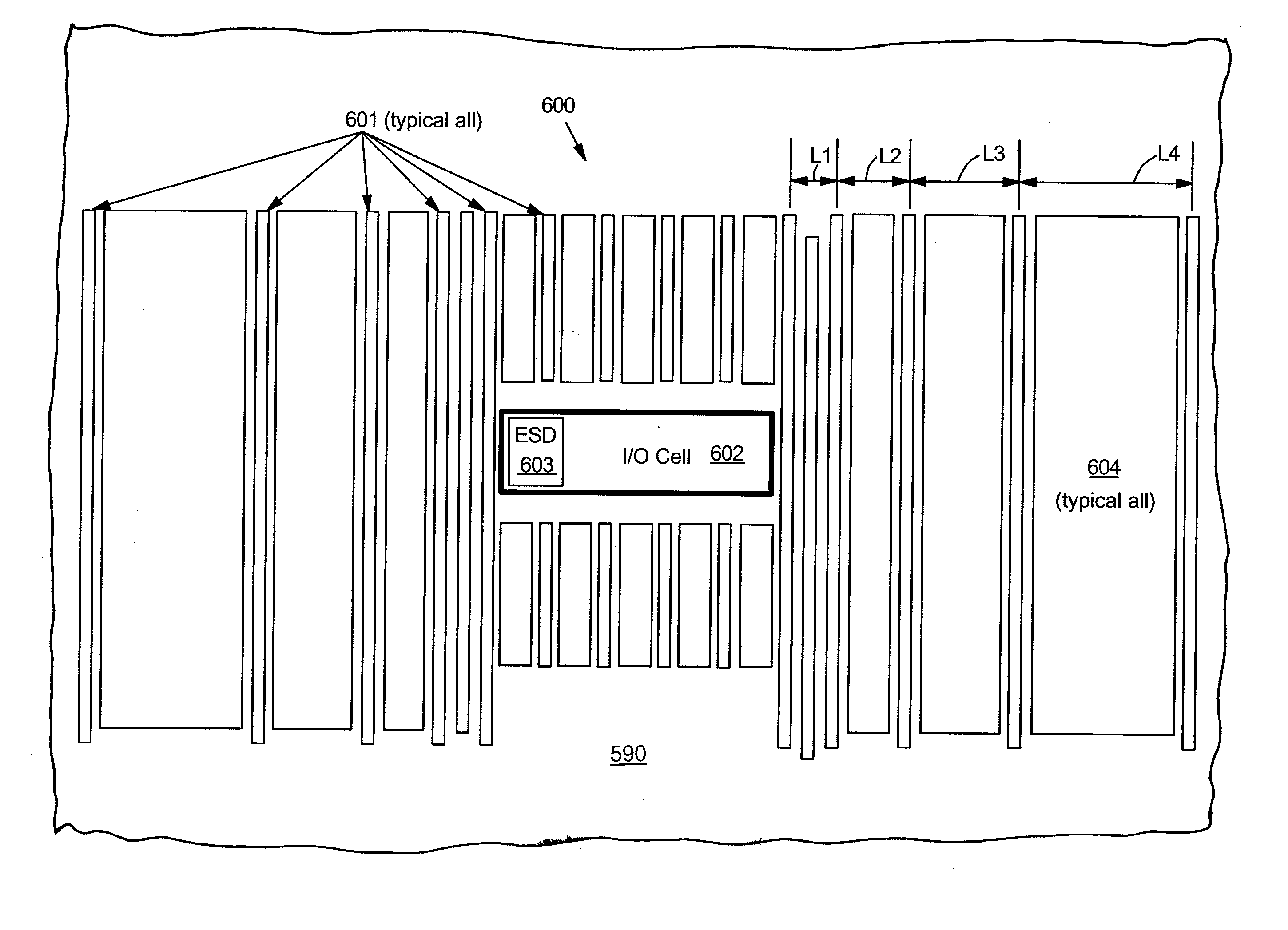
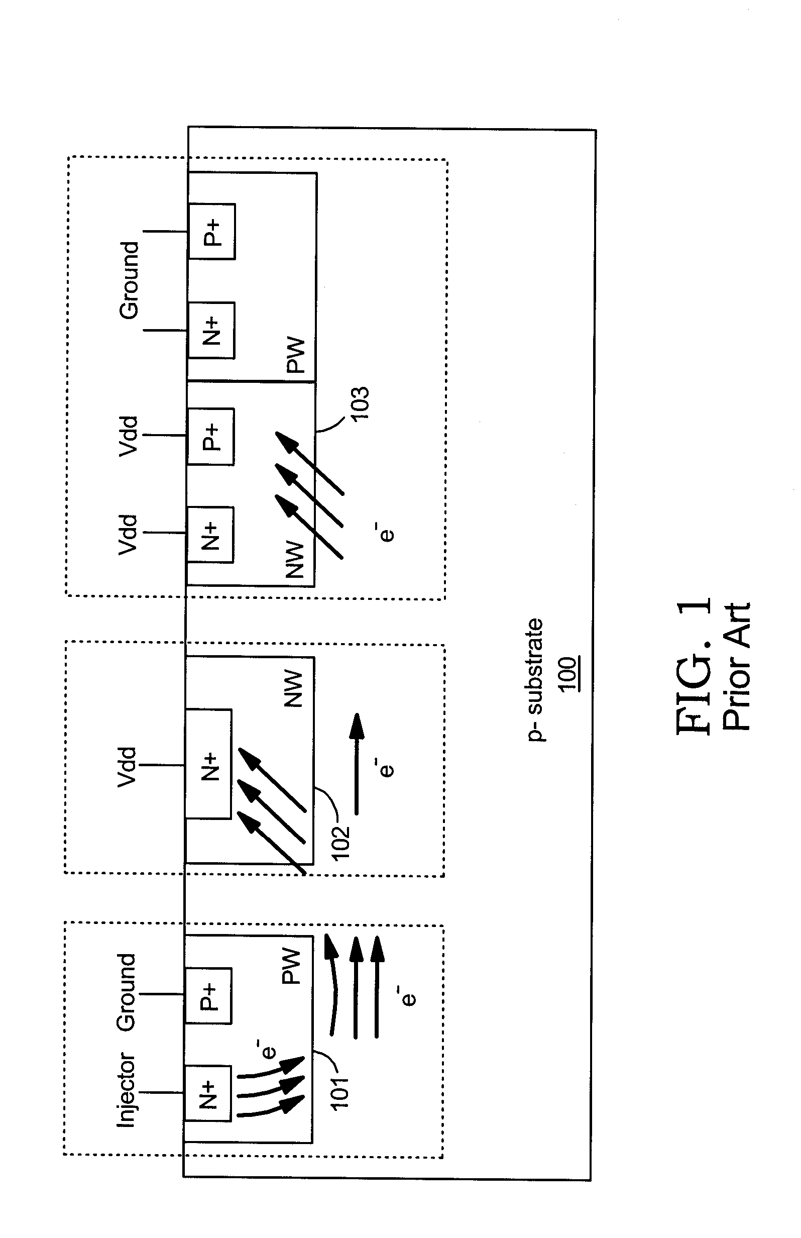
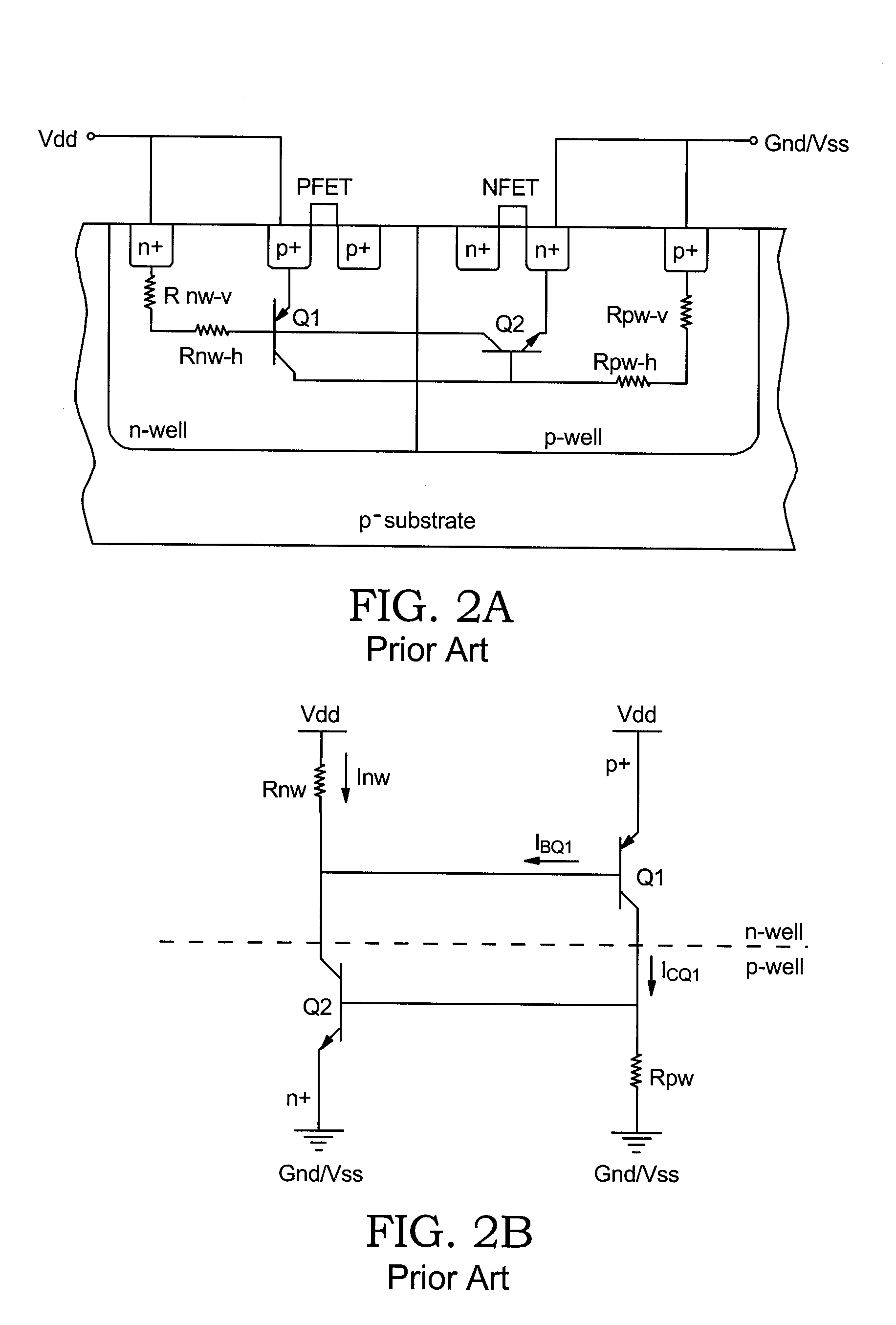
[0037] The present invention relates to a method and structure for suppression of latch-up within integrated circuits. Injection of carriers into an IC can arise at any point of conduction on the IC and can originate from a variety of sources. Regardless of injection source and location, the density of injected carriers will be greatest within the region of the IC near the location of injection, i.e. the injection site. It is in the region near the injection site where protection against latch-up should be the most robust. As distance is traversed away from the location of current injection, however, there will be fewer carriers available to cause a latch-up condition. Thus, the latch-up protection strategy remote from the injection source need not be as robust as it need be nearer the injection source, yet maintaining latch-up robustness for a given injection of current.

[0038] In terms of electrical variables, a latch-up condition can occur when the injected current, for example, ...


PUM


Abstract

A method and structure for protection against latch-up is provided. Integrated circuits manufactured in accordance with the present disclosure feature well and substrate contacts of varying periodicity. Such a strategy enables maximizing the design of an integrated circuit as to the suppression of latch-up while concurrently optimizing available area on the chip allocable to circuit design. This method and structure is particularly beneficial to protect against cable discharge events and other discharge occurrences prone to injecting large current densities into an integrated circuit.

Description

BACKGROUND OF INVENTION [0001] 1. Field of the Invention [0002] The present invention relates generally to latch-up protection for integrated circuits, and more particularly to the strategic placement of n-well, p-well or substrate contacts for external latch-up robustness. [0003] 2. Background of the Invention [0004] Advances in modern integrated circuit (IC) technology have enabled MOS devices to be made with ever thinner gate oxides using submicron complementary metal oxide semiconductor (CMOS) technology. Use of thinner gate oxides, however, results in devices that are increasingly susceptible to failure arising from electrical overstress / electrostatic discharge (EOS / ESD) events. Such failures can result in the immediate failure of the device, circuit or system. [0005] To reduce the destructiveness of an ESD event, IC designers incorporate protective circuits within their IC layouts to dissipate the energy of a discharge. Such ESD protection circuitry is typically located at or ...

Claims


Application Information

Patent Timeline
IPC IPC(8): H01L27/092
CPCH01L27/0921
Inventor CHATTY, KIRAN V.COTTRELL, PETER E.GAUTHIER, ROBERT J. JR.MUHAMMAD, MUJAHID
Owner IBM CORP
Why Eureka
Try Eureka