System & method for performing design rule check

a design rule and system technology, applied in the field of systems, can solve the problems of logic rule errors, sizing, requiring a large spacing, etc., and achieve the effect of eliminating false errors

Inactive Publication Date: 2005-04-21
UNITED MICROELECTRONICS CORP
View PDF17 Cites 27 Cited by
  • Summary
  • Abstract
  • Description
  • Claims
  • Application Information

AI Technical Summary

Benefits of technology

[0012] An object of the present invention, therefore, is to provide a design rule checking system and method that accurately reports appropriate errors for appropriate regions in a system that includes two different kinds of circuits, i.e., such as memory and logic.
[0013] A related object is to eliminate false errors caused by design rule checking tools examining regions that are not subject to the same design rules supported by the design rule-checking tool.
[0014] These objects are achieved by the present invention, which provides a system and method of

Problems solved by technology

For some types of ICs, this process of checking the design errors can be automated, but for many others, it cannot.
These systems present a unique challenge to the design process, because memory and logic circuits have different sizing, performance and scaling issues when embodied in silicon.
The false logic rule errors 252 are caused by the fact that logic circuits implemented in silicon typically require greater spacings, sizings and margins than memory circuits.
This can be extremely time consuming and cumbersome since the number of false design rule errors will increase relative to the number of memory blocks used and the siz

Method used


Image

  • System & method for performing design rule check
  • System & method for performing design rule check
  • System & method for performing design rule check

Examples


Embodiment Construction

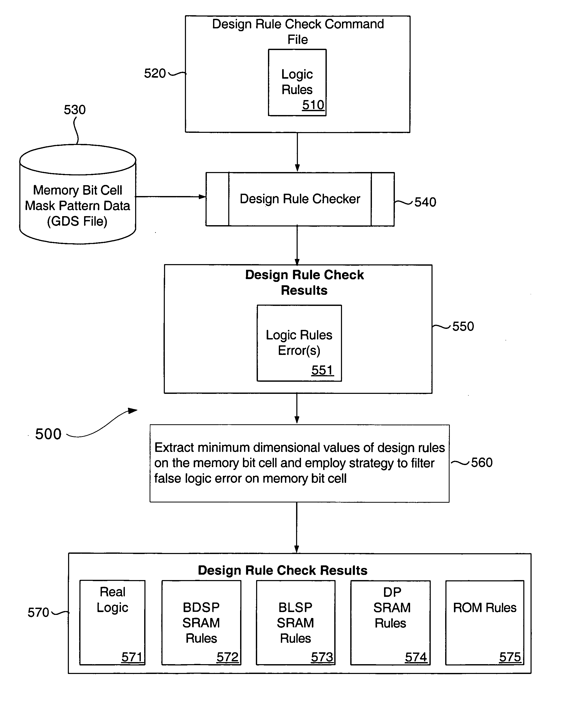
[0028] The present invention provides a solution to the disadvantages of the first and second conventional methods of checking design rules as explained above. From a broad perspective, the method generally applies the right set of rules to the right regions of the mask pattern data. To simplify the process (i.e., to avoid having to create an entire set of design rule checks from scratch, or to harmonize several different types of design rules from different memory cell vendors) and ensure its accuracy with respect to any particular set of foundry rules, the customized design rules are based on modifying a standard set of Logic Rules as needed to reflect needs of particular regions in the chip. Thus, a customized design rule is created for each different type of region that may be present on the chip, and this customized design rule is in fact simply based on pushing more liberal parameters onto stricter parameters contained in the standard Logic rules, and only in circumstances whe...


PUM


Abstract

An improved system and method is disclosed for performing a design rule check on a proposed integrated circuit (IC) layout, and for creating customized design rule check command files. The individual layers of the IC (a system on chip—SOC) are separated into different regions having different kinds of features (i.e., memory or logic). Each different type of region is then analyzed in accordance with the customized design rule command file so that so-called “false errors” are eliminated. The invention thus improves, among other things, a development time for getting a design implemented in silicon.

Description

RELATED APPLICATION DATA [0001] The present application claims priority from provisional application Ser. No. 60 / 278,672 filed Mar. 20, 2001, which is also incorporated by reference herein.FIELD OF THE INVENTION [0002] The present invention relates to the field of semiconductor design technology, and in particular, to systems and techniques used for implementing circuit designs into silicon based integrated circuits (ICs). BACKGROUND [0003] In the field of semiconductor design technology, a design rule check (DRC) is a well-known process for inspecting whether mask pattern data of a semiconductor integrated circuit is correctly designed in compliance with fabricators' topological layout rules (TLR). The TLR are unique to each fabrication facility, or semiconductor wafer plant, based on available process technologies, equipment limitations, etc. An example of prior art DRC system is illustrated in U.S. Pat. No. 6,063,132 incorporated by reference herein. [0004] Integrated circuit des...

Claims


Application Information

Patent Timeline
IPC IPC(8): G06F17/50
CPCG06F17/5081G06F30/398
Inventor TEH, CHEEHOELAM, NIMCHOTRUONG, MAU
Owner UNITED MICROELECTRONICS CORP
Why Eureka
Try Eureka