Signal transmitting device suited to fast signal transmission

a signal transmission and signal technology, applied in the field of signal transmission devices suited to fast signal transmission, can solve the problems of waveform distortion on the transmission line, receivers not being able to recognize high level, reflection of signal, etc., to reduce line impedance, reduce transmission line amplitude, and quickly transmit signal

Inactive Publication Date: 2005-04-28
LG ELECTRONICS INC
View PDF17 Cites 20 Cited by
  • Summary
  • Abstract
  • Description
  • Claims
  • Application Information

AI Technical Summary

Benefits of technology

[0027] It is an object of the present invention to provide a signal transmitting device, a circuit block, and an integrated circuit which are arranged to overcome the foregoing disadvantages, suppress the drop of a signal potential on a transmission line having branched lines, prevent repetitive reflections in each branched line, and keep an amplitude of a signal small on the line, for quickly transmitting a signal.
[0031] In accordance with the present invention, by inserting a resistor having a resistance close to a value derived by reducing a half of an impedance of the line from the impedance of the branched line, it is possible to prevent repetition of reflections inside of the branched line and attenuate the amplitude of the transmission line by dividing the inserted resistance and the terminating resistance, thereby enabling to quickly transmit the signal.
[0032] In the case where a large number of branch points exist on the inter-block transfer line, the capacitance because of the existence of the resistors, the inter-block transmission line is not able to see the branched line directly (i.e., the total of the transmission line load capacitance and the capacitance of the driving and receiving circuits). This is effective in suppressing the line impedance from being lowered. Further, the waveform distortion due to live-insertion can be suppressed.

Problems solved by technology

Hence, the mismatch of the forward synthesized impedance 25Ω to the impedance of 50Ω of the transmission line on which the signal has passed results in bringing about the reflection of the signal.
Eventually, after repeated signals, the level of voltage at points B, C and D will increase to levels much closer to the level at point A, but, until this occurs, the receivers will not be able to recognize the High level.
This brings about a waveform distortion on the transmission line 100.
This results in disadvantageously increasing the delay time, and thereby prevents quickly transmitting the signal.
This also results in disadvantageously distorting the signal waveform, thereby lowering the reliability of the signal transmission.
The special value given to the on resistance as mentioned in the paper, however, makes the widely available transistors having an on resistance of about 10 W useless.
Further, such a higher on resistance given to the sending circuit 21 leads to increasing the power consumption of the driving circuit, thereby disadvantageously increasing the overall power consumption.
The signal reflection may disadvantageously inhibit the realization of fast signal transmission.
That is, this technique does not define any resistance based on a relation of an impedance between the inter-block signal transmission line and the signal transmission line inside of the block.
As in the previously described arrangement, this signal reflection may disadvantageously inhibit realization of fast signal transmission.

Method used


Image

  • Signal transmitting device suited to fast signal transmission
  • Signal transmitting device suited to fast signal transmission
  • Signal transmitting device suited to fast signal transmission

Examples


embodiment 2

[0100] The following description will be directed to embodiment 2 in which the present invention is applied to a bidirectional transmission line.

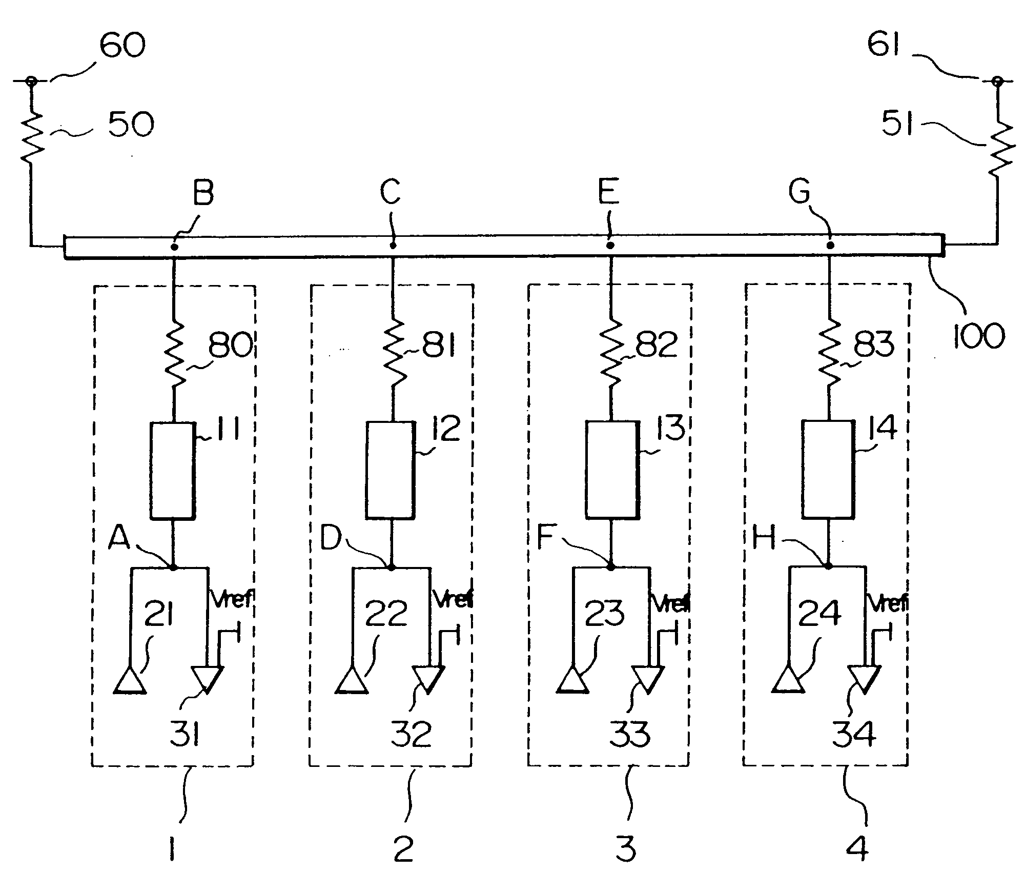
[0101]FIG. 11 is a fundamental block diagram showing the second embodiment. The circuit blocks 1 to 4 provide driving circuits 21 to 24, receiving circuits 31 to 34, resistors 80 to 83, and transmission lines 11 to 14, respectively. A transmission line 100 is connected to the circuit blocks 1 to 4 and is terminated by the resistors 50 and 51, each having a resistance equal to a characteristic impedance value of the transmission line 100.

[0102]FIG. 11 shows the transmission line terminated at both ends by the resistors. However, if desired, the transmission bus may be terminated at one end by one resistor. Further, FIG. 11 shows four blocks. In actuality, the present invention may apply to any transmission line if it is connected to two or more blocks.

[0103] The arrangements of the driving circuits 21 to 24 and the receiving circuits 31 t...

embodiment 3

[0113] The following description will be directed to a third embodiment which is particularly effective in the case of providing a large capacitance at the tip of each branched line in a situation where there are many branched lines. FIG. 14 is a fundamental block diagram for explaining a unidirectional transmission bus according to this embodiment. FIG. 15 is a fundamental block diagram for explaining a bidirectional transmission bus according to this embodiment. In FIG. 14, a circuit block 1 includes a driving circuit 21, and circuit blocks 2 to 4 include receiving circuits 32 to 34, respectively. Further, the blocks have resistors 80 to 83 and transmission lines 11 to 14, respectively. In FIG. 15, the circuit blocks 1 to 4 provide sending circuits 21 to 24, receiving circuits 31 to 34, resistors 80 to 83, and transmission lines 11 to 14, respectively. In FIGS. 14 and 15, the transmission line 100 is connected to the circuit blocks 1 to 4, and is terminated by resistors 50 and 51 ...

embodiment 4

[0131]FIG. 27 shows an embodiment in which the driving circuit and the receiving circuit are integrated so that an inter-circuit block transmission line is connected to an intra-circuit block transmission line through an transmission bus like a lead of an integrated circuit.

[0132] In FIG. 27, a numeral 5 denotes an inner circuit block (an inner unit, for example, an integrated circuit) which is mounted on a circuit block 1 (for example, a board having an integrated circuit mounted thereon). Numerals 6 to 8 denote inner circuit blocks having receiving circuits 32 to 34, respectively, which inner circuit blocks are mounted inside of the circuit blocks 2 to 4, respectively. The circuit blocks 1 to 4 have resistors 80 to 83 and transmission lines 11 to 14 and 41 to 44, respectively. The transmission lines 11 to 14 are designed to have the same or almost the same characteristic impedance as that of the transmission lines 41 to 44. Further, the transmission line 100 has the circuit block...


PUM


Abstract

A signal transmitting circuit includes a circuit block having a driving circuit and an intra-block transmission line for transmitting a signal from the driving circuit, a circuit block having a receiving circuit and an intra-block transmission line for transmitting the signal to said receiving circuit, and a main interblock transmission line for propagating a signal between the driving and receiving circuit blocks. The inter-block transmission line is terminated by a resistor having substantially the same impedance as the interblock transmission line. The intra-block transmission lines are provided with a resistance element having a resistance substantially equal to a value derived by subtracting half of an impedance of the inter-block transmission line from an impedance of the intra-block transmission line, to lower signal amplitude and suppress reflections of a signal at branch points along the main interblock transmission line, thereby enabling a high-speed signal transfer.

Description

BACKGROUND OF THE INVENTION [0001] The present invention relates to technique of transmitting a signal between elements such as a CPU and a memory device or memory IC (for example, between digital circuits each composed of CMOS elements or functional blocks of CMOS elements), and, more particularly to techniques of quickly transmitting a signal through one bus in which one main transmission line has plural elements connected thereto. [0002] As a technique of quickly transmitting a signal between digital circuits each composed of a semiconductor integrated circuit, there has been proposed a technique of a low-amplitude interface for propagating a signal having a signal amplitude as low as about 1 volt. [0003] As a representative example of such a low-amplitude interface, a GTL (Gunning Transceiver Logic) interface or a CTT (Center Tapped Termination) interface has been heretofore proposed. These low-amplitude interfaces are discussed in detail in pp 269 to 290 of Nikkei Electronics, ...

Claims


Application Information

Patent Timeline
Patent Type & Authority Applications(United States)
IPC IPC(8): G06F3/00G06F12/00G06F13/16G06F13/40G11C11/401H03K19/0175H04B3/02H04L25/02H05K1/02H05K1/14
CPCG06F13/4072G06F13/4086H04B3/02H04L25/0278H05K1/14H04L25/0292H04L25/0298H05K1/0216H05K1/0237H04L25/028
Inventor TAKEKUMA, TOSHITSUGUKURIHARA, RYOICHIYAMAGIWA, AKIRA
Owner LG ELECTRONICS INC
Why Eureka
Try Eureka