Processing apparatus and method

a technology of dangling bond and processing method, which is applied in the direction of packaging, electric discharge tubes, edible oils/fats, etc., can solve the problems of requiring a long time for treatment, affecting device performance or operation, and disadvantageously having a low dangling bond termination speed, so as to achieve efficient termination and minimize plasma damage

Inactive Publication Date: 2005-04-28
CANON KK
View PDF6 Cites 141 Cited by
  • Summary
  • Abstract
  • Description
  • Claims
  • Application Information

AI Technical Summary

Benefits of technology

[0006] Accordingly, it is an exemplary object of the present invention to provide a process

Problems solved by technology

It has been known that a semiconductor device includes dangling bonds in a thin film interface in a silicon system material, a polycrystal silicon grain boundary, and a defect that results from plasma damages, and the dangling bonds negatively affe

Method used


Image

  • Processing apparatus and method
  • Processing apparatus and method
  • Processing apparatus and method

Examples


first embodiment

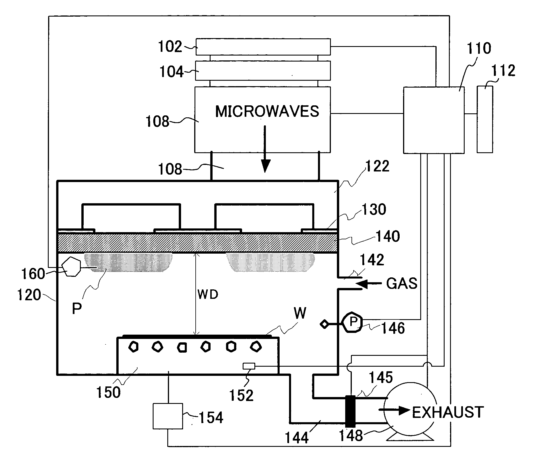
[0043] This embodiment used the processing apparatus 100 and the above processing method to hyrically terminate poly-Si TFT formed on a quartz substrate. The working distance WD between the dielectric window 140 and the susceptor 150 was set 100 mm, and the process conditions set the substrate temperature to be 275° C., gas to be 100% hydrogen, the gas pressure to be 66.5 Pa, and the microwave output to be 3 kW. As a result, only tem-minute treatment could not only provide effects, such as a S-value reduction effect, similar to that of the conventional RIE apparatus working for 30 minutes, but also restrain damages to the device in a low or indifferent level.

[0044] Thus, the processing apparatus 100 forms the high-density plasma only near the dielectric window 140, and provides a plasma treatment to the object W using diffusions from the high-density plasma, without exposing the object W to the plasma generating region P. In addition, the processing apparatus 100 does not apply bia...


PUM


Abstract

A processing method that uses process gas plasma that contains at least hydrogen to terminate dangling bonds in an object that at least partially contains a silicon system material includes the steps of placing the object on a susceptor in a process chamber that includes a dielectric window and the susceptor, and controlling a temperature of the susceptor to a predetermined temperature, controlling a pressure in the process chamber to a predetermined pressure, introducing the process gas into the process chamber, and introducing, via the dielectric window, microwaves for a plasma treatment to the object into the process chamber so that plasma of the process gas has plasma density of 1011 cm−3 or greater, wherein a distance between the dielectric window and the object is maintained between 20 mm and 200 mm.

Description

[0001] This application claims a benefit of priority based on Japanese Patent Application No. 2003-362535, filed on Oct. 22, 2003, which is hereby incorporated by reference herein in its entirety as if fully set forth herein. BACKGROUND OF THE INVENTION [0002] The present invention relates generally to a semiconductor device manufacture, and more particularly to a plasma processing method and apparatus for terminating dangling bonds. [0003] It has been known that a semiconductor device includes dangling bonds in a thin film interface in a silicon system material, a polycrystal silicon grain boundary, and a defect that results from plasma damages, and the dangling bonds negatively affect device performance or operations, such as carrier trap level and barriers to carrier movements. For example, it has also been known that the dangling bonds in a poly-silicon grain boundary attenuate ON current, increase OFF current and S value in a thin film transistor (“TFT”), and the defects betwee...

Claims


Application Information

Patent Timeline
IPC IPC(8): H01L21/30H01L21/302H01L21/304H01L21/306H01L21/205H01L21/322H01L21/336H01L29/786
CPCH01J37/32192H01L21/306H01L21/3003A23D9/06B65D81/2023
Inventor ISHIHARA, SHIGENORI
Owner CANON KK
Why Eureka
Try Eureka