Self-Aligned Field Plate Mesa FPM SiC Schottky Barrier Diode

a field plate and barrier diode technology, applied in the direction of diodes, semiconductor devices, electrical equipment, etc., can solve the problems of high difficulty in design of high-performance floating field ring termination, high breakdown voltage vbr, and difficulty in ion implantation in wide-bandgap materials. achieve the effect of high breakdown voltage and high precision

Pending Publication Date: 2021-01-21
HITACHI ENERGY SWITZERLAND AG
View PDF8 Cites 1 Cited by
  • Summary
  • Abstract
  • Description
  • Claims
  • Application Information

AI Technical Summary

Benefits of technology

[0025]As in the method of the invention areas in the termination region that are exposed by the field plate are etched in the step of anisotropic etching, an outer circumferential edge of the field plate is self-aligned with a sidewall of the first recess formed in the step of anisotropic etching. The recess formed in the step of anisotropic etching forms a mesa edge termination thus an edge termination by a process free of any implantation step. The field plate protects areas of the wide-bandgap semiconductor layer that shall not be etched during the step of anisotropic etching. Accordingly, a deep SiC etch can be performed more reliably and the sidewall of the first recess and the circumferential edge of the field plate are mutually aligned in lateral direction with high precision. Consequently, as it is discussed above, because of the precise alignment, the electric field crowding below the circumferential edge of the field plate can be efficiently reduced by the mesa edge termination thus resulting in a device providing higher breakdown voltage.
[0026]Using a patterned metal layer as the field plate and as an etching mask in the step of anisotropic etching is advantageous compared to using an etching mask made of photoresist because metal is more resistant to etchants, that are used in the step of anisotropic etching of the wide-bandgap semiconductor layer, than photoresist. As discussed above, using the dielectric layer between the wide-bandgap semiconductor layer and the field plate amplifies the effect of the field plate and provides additional electric field relief.

Problems solved by technology

However, high power semiconductor devices based on wide-bandgap semiconductor materials require an efficient edge termination to avoid electric field crowding at the edge of the main contact resulting in breakdown of the device at a relatively low breakdown voltage VBR.
On the other hand, the design of a high performance floating field ring termination is very challenging given the high number of factors (e.g. ring spacing) affecting the most important trade-off between breakdown voltage and occupied wafer area.
However, ion implantation in wide-bandgap materials is more difficult than in conventional semiconductor materials.
Moreover, the implantation steps require high temperature implantation facilities and an annealing oven especially designed for activation of such wide-bandgap materials, which makes the fabrication comparably costly.
There however, due to the increasing electric field crowding, the risk of dielectric failure increases, thus limiting the achievable electrical breakdown voltage.
In high power devices the problem of dielectric failure is more pronounced than in conventional silicon devices as the critical electric field crowding is almost one order of magnitude larger than in conventional silicon devices.
Nevertheless premature breakdown occurs before an ideal breakdown voltage is achieved.

Method used


Image

  • Self-Aligned Field Plate Mesa FPM SiC Schottky Barrier Diode
  • Self-Aligned Field Plate Mesa FPM SiC Schottky Barrier Diode
  • Self-Aligned Field Plate Mesa FPM SiC Schottky Barrier Diode

Examples


first embodiment

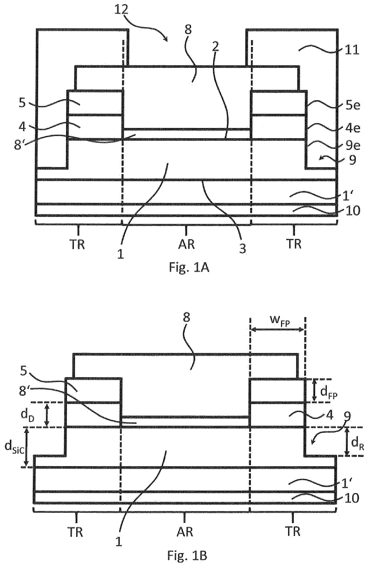
[0050]Referring to FIGS. 1A and 1B, an exemplary embodiment according to the invention comprises an n-type silicon carbide (SiC) layer 1, an n+-type SiC substrate 1′, a dielectric layer 4, a field plate 5, a first recess 9, a backside electrode 10, a frontside electrode (contact electrode 8) and a passivation layer 11.

[0051]The SiC layer 1 (an example of the wide-bandgap semiconductor layer 1 in the claims) is formed on the SiC substrate 1′, has exemplarily a relatively low doping concentration of 1017 cm−3 or less and forms the drift layer in the final power semiconductor device. The SiC substrate 1′ has, for example, a higher doping concentration of 1018 cm−3 or more and is formed on the backside electrode 10. Appropriate doping profiles of the SiC layer 1 and the SiC substrate 1′ for use in a Schottky diode are well known in the prior art. The SiC layer 1 has a first main side 2 and a second main side 3. The first main side 2 and the second main side 3 extend in a lateral directi...

second embodiment

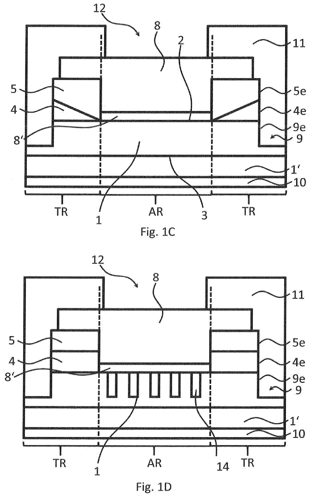
[0059]A second embodiment according to the invention is described with reference to FIG. 1C. Due to the many similarities between the first embodiment and the second embodiment only differences of the first embodiment to the second embodiment are discussed. The remaining features are the same as in the first embodiment and for an explanation thereof it is referred to the first embodiment discussed above with reference to FIGS. 1A to 1B. In contrast to the first embodiment, dielectric layer 4 is formed such that its thickness do increases with increasing lateral distance from the active region AR. The thickness do may increase from a first value to a second value. The thickness may increase continuously from a first value to a second value. The angle between the straight line connecting the first value and the second value and a plane parallel to the first main side may be in the range between 0.1° and 90°, exemplarily between 1° and 10°, more exemplarily between 1° and 5°. The first...

third embodiment

[0060]A third embodiment according to the invention is described with reference to FIG. 1D. Due to the many similarities between the first embodiment and the third embodiment only differences of the first embodiment to the third embodiment are discussed. The remaining features are the same as in the first embodiment and for an explanation thereof it is referred to the first embodiment discussed above with reference to FIGS. 1A and 1B. The third embodiment differs from the first embodiment in that the active region AR of the SiC layer 1 also comprises at least one second recess 14 which has the same depth as the first recess 9 in the termination region TR. The at least one second recess 14 is filled with some filling material, for example insulating material such as a dielectric material or an oxide. This configuration may have a positive effect on leakage currents. The third embodiment may also have the dielectric layer 4 with increasing thickness as shown in the second embodiment.

M...


PUM

PropertyMeasurementUnit
depthaaaaaaaaaa
depthaaaaaaaaaa
thicknessaaaaaaaaaa

Abstract

A power semiconductor device includes a wide-bandgap semiconductor layer having an active region and a termination region that laterally surrounds the active region. The wide-bandgap semiconductor layer has a first recess that is recessed from the first main side in the termination region and surrounds the active region and a second recess that is recessed from the first main side in the active region and is filled with an insulating material. A depth of the second recess is the same as a depth of the first recess. A field plate on the first main side of the wide-bandgap semiconductor layer exposes a first portion of the wide-bandgap semiconductor layer in the termination region.

Description

FIELD OF THE INVENTION[0001]The present invention relates to a wide-bandgap high power semiconductor device with effective edge termination comprising a field plate and a recess in the termination region (mesa termination structure) and to a method for manufacturing the same.BACKGROUND OF THE INVENTION[0002]Wide-bandgap (WBG) semiconductor materials such as silicon carbide (SiC), gallium nitride, gallium oxide, boron nitride, aluminum nitride, zinc oxide, diamond etc. allow to make semiconductor devices more powerful and energy efficient than those made from conventional semiconductor materials.[0003]However, high power semiconductor devices based on wide-bandgap semiconductor materials require an efficient edge termination to avoid electric field crowding at the edge of the main contact resulting in breakdown of the device at a relatively low breakdown voltage VBR.[0004]Edge termination may be provided in various ways including floating field rings, junction termination extension (...

Claims


Application Information

Patent Timeline
Patent Type & Authority Applications(United States)
IPC IPC(8): H01L29/40H01L29/06H01L29/16H01L29/66H01L29/872H01L29/20H01L29/861
CPCH01L29/407H01L29/0649H01L29/0661H01L29/1608H01L29/8613H01L29/66143H01L29/872H01L29/2003H01L29/6606H01L29/1602H01L29/24H01L29/402H01L29/66212H01L29/8083
Inventor MIHAILA, ANDREIKNOLL, LARSKRANZ, LUKAS
Owner HITACHI ENERGY SWITZERLAND AG
Why Eureka
Try Eureka