Interfacing multiple wavelength sources to thin optical waveguides utilizing evanescent coupling

a technology of evanescent coupling and optical signal, applied in the field of system and methodology for coupling multiple wavelength optical signal, can solve the problems of inability to efficiently coupling a relatively large range of wavelengths into a relatively thin surface waveguide layer, the grating structure of the rigrod is limited to diffracting, and the problem of light coupling into and out of the planar waveguide structur

Active Publication Date: 2005-05-05
CISCO TECH INC
View PDF5 Cites 45 Cited by
  • Summary
  • Abstract
  • Description
  • Claims
  • Application Information

AI Technical Summary

Benefits of technology

[0010] In formation, the grating may be formed at the interface between an evanescent coupling layer and the silicon surface waveguide, at the interface between the prism coupler and the evanescent coupling layer, or even etched within the surface of the silicon waveguide or prism coupler. Another material (for example, silicon dioxide) may be added to “fill” an etched grating, where the difference in refractive index between the “fill” and the grating is used to determine the effective refractive index. In one exemplary embodiment, silicon nitr...

Problems solved by technology

One issue associated with the use of optoelectronic integrated circuits is the problem of coupling light into and out of a planar waveguide structure, particularly a relatively thin (i.e., sub-micron) waveguide structure.
Moreover, the grating structure of Rigrod is found to be limited to diffracting a first-order mode of the light beam and is generally used for steering a particular input signal beam.
As a result, this Rigrod structure remains incapable of efficiently coupling a relatively large...

Method used


Image

  • Interfacing multiple wavelength sources to thin optical waveguides utilizing evanescent coupling
  • Interfacing multiple wavelength sources to thin optical waveguides utilizing evanescent coupling
  • Interfacing multiple wavelength sources to thin optical waveguides utilizing evanescent coupling

Examples


Embodiment Construction

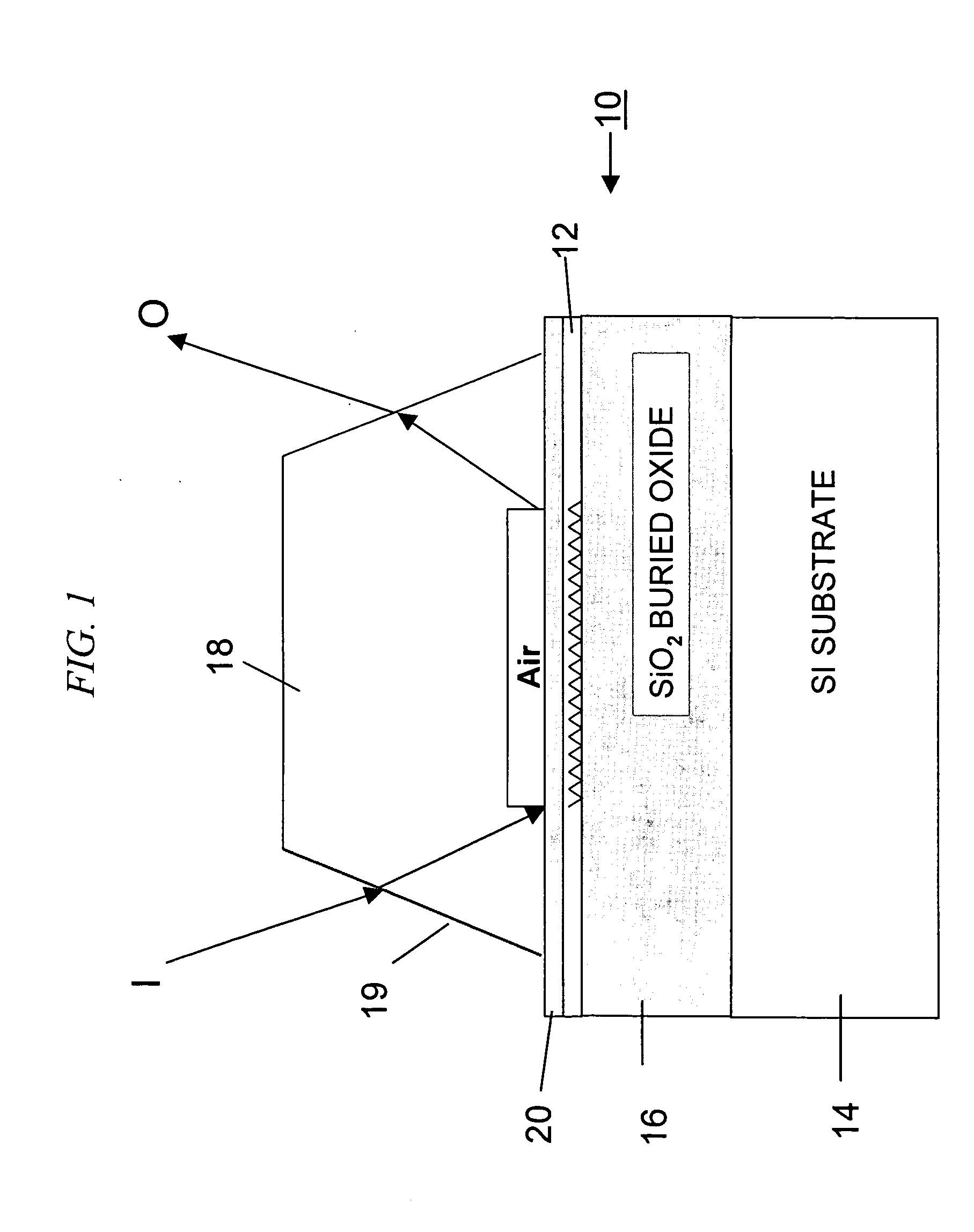
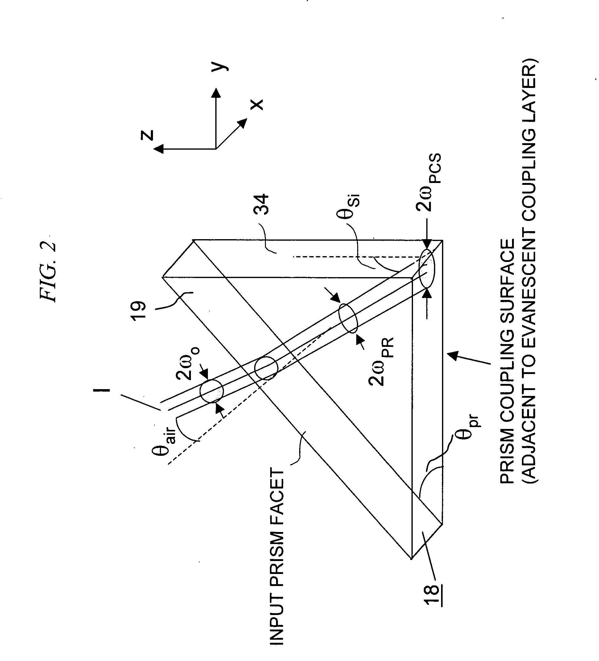
[0025] An exemplary arrangement utilizing prism coupling to bring light into and out of a relatively thin silicon waveguide is illustrated in FIG. 1. In this particular example, an SOI wafer 10 includes a relatively thin (sub-micron) silicon waveguide layer 12 that is separated from a silicon substrate 14 by a buried oxide layer 16. A prism coupling device 18 is utilized to couple an external lightwave beam I into silicon waveguide layer 12, as shown. An evanescent coupling layer 20, disposed between silicon waveguide layer 12 and prism coupling device 18 is used in this case to affect the coupling between the components. As discussed in our co-pending applications, the refractive index of evanescent coupling layer 20 is selected to be less than the indexes of prism coupler 18 and silicon waveguide 12 so that efficient guiding within waveguide layer 12 is achieved and maintained. Both prism coupling device 18 and SOI wafer 10 are preferably fabricated using conventional wafer-level ...


PUM


Abstract

An arrangement for achieving and maintaining high efficiency coupling of light between a multi-wavelength optical signal and a relatively thin (e.g., sub-micron) silicon optical waveguide uses a prism coupler in association with an evanescent coupling layer. A grating structure having a period less than the wavelengths of transmission is formed in the coupling region (either formed in the silicon waveguide, evanescent coupling layer, prism coupler, or any combination thereof) so as to increase the effective refractive index “seen” by the multi-wavelength optical signal in the area where the beam exiting/entering the prism coupler intercepts the waveguide surface (referred to as the “prism coupling surface”). The period and/or duty cycle of the grating can be controlled to modify the effective refractive index profile in the direction away from the coupling region so as to reduce the effective refractive index from the relatively high value useful in multi-wavelength coupling to the lower value associated with maintaining confinement of the optical signals within the surface waveguide structure, thus reducing reflections along the transition region.

Description

CROSS-REFERENCE TO RELATED APPLICATION [0001] The present application claims the priority of Provisional Application No. 60 / 500,184 filed Sep. 4, 2003.TECHNICAL FIELD [0002] The present invention relates to a system and methodology for coupling multiple wavelength optical signals to a relatively thin silicon surface waveguide and, more particularly, to the use of an evanescent coupling region to achieve multiple wavelength coupling. DESCRIPTION OF THE PRIOR ART [0003] To meet the bandwidth requirements of current and future high speed communication applications, state-of-the-art telecommunication components and systems must provide a host of sophisticated signal processing and routing functions, in both the optical and electronic domains. As the complexity level increases, the integration of more functions and components within a single package becomes required to meet various system-level requirements and reduce the associated size and cost of the complete system. It has been recog...

Claims


Application Information

Patent Timeline
IPC IPC(8): G02BG02B6/34
CPCG02B6/12007G02B6/34G02B6/124
Inventor GHIRON, MARGARETGOTHOSKAR, PRAKASHMONTGOMERY, ROBERT KEITHPATEL, VIPULKUMARPATHAK, SOHAMSHASTRI, KALPENDUYANUSHEFSKI, KATHERINE A.
Owner CISCO TECH INC
Why Eureka
Try Eureka