Heat treatment for edges of multilayer semiconductor wafers

a multi-layer semiconductor and heat treatment technology, applied in drying, drying machines, light and heating apparatus, etc., can solve the problems of oxidizing the surface of the wafer, drawbacks of annealing operations, annealing operations, etc., to prevent the appearance of slip lines, modify the heat absorption coefficient of the wafer, and prevent deformation of the wafer

Inactive Publication Date: 2005-05-05
SOITEC SA
View PDF11 Cites 6 Cited by
  • Summary
  • Abstract
  • Description
  • Claims
  • Application Information

AI Technical Summary

Benefits of technology

[0016] Presented is a method for heat treating a multilayer semiconductor wafer having a central region and a peripheral edge each having a surface. The method includes selecting thickness values for the layers of the wafer to provide substantially equivalent heat absorption coefficients both in the central region and the edge of the wafer, so that a substantially equivalent temperature is attained over the surface of the central region and the peripheral edge during thermal treatment, to thus prevent the appearance of slip lines on those surfaces while also preventing deformation of the wafer due to the thermal treatment. To achieve the desired thickness, layers or portions of layers can be selectively added or otherwise provided upon the central region or peripheral edge of the wafer, or on both, to modify the heat absorption coefficient of the wafer.

Problems solved by technology

Such annealing, which is performed under an oxidizing atmosphere, oxidizes the surface of the wafer.
It has been observed that drawbacks are associated with annealing operations performed on such wafers.
More precisely, RTP type annealing operations (including RTA, RTO, and the like.) generate defects known as “slip lines” in wafers.
This phenomenon of slip lines at the periphery of the wafer is particularly severe for multilayer wafers having an edge.
RTP type annealing thus tends to generate slip lines, and this drawback is in particular severe for multilayer semiconductor wafers having an edge.
Such heat treatments subject the wafer to very high levels of thermal stress because of the very rapid temperature rises they induce.
It should be understood that this major drawback is more severe when annealing is performed by radiating heat from one or more heat sources.
Therefore, there are several drawbacks when annealing is performed on multilayer semiconductor wafers that include an edge.
However, the documents do not seek to solve the particular problem mentioned above.
Such documents are generally limited to treating simple single-layer wafers without edges, where the specific problem of generating slip-lines on multilayer wafers having an edge does not arise.
However the teaching of those documents is limited to setting up a thermal continuity ring in order to avoid edge effects which do not correspond to the specific problem mentioned above.
Furthermore, none of those documents even mentions problems associated specifically with multilayer wafers.

Method used


Image

  • Heat treatment for edges of multilayer semiconductor wafers
  • Heat treatment for edges of multilayer semiconductor wafers
  • Heat treatment for edges of multilayer semiconductor wafers

Examples


Embodiment Construction

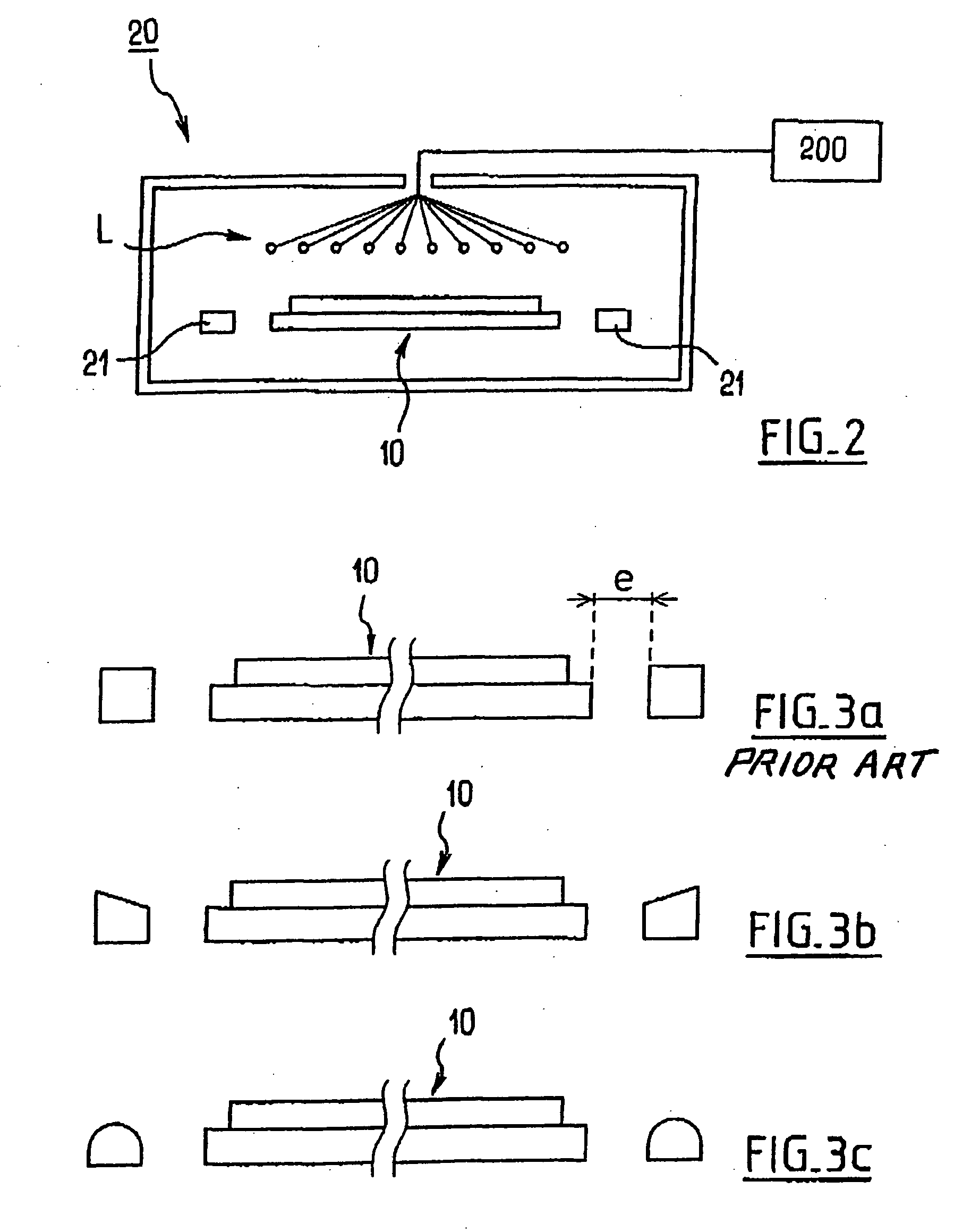
[0029] With reference initially to FIG. 2, an annealing installation 20 is shown for performing annealing process on a wafer 10 that includes an edge. This installation is suitable for performing RTP type annealing, which may be annealing for smoothing purposes. This type of installation has been selected to illustrate the invention since the drawbacks generated by such annealing (slip lines, and other drawbacks) are particularly severe.

[0030] A particularly advantageous application of the invention thus concerns that use of RTP type annealing, such as RTO annealing, or RTA type finishing annealing for smoothing the surface of the wafer. Nevertheless, the present invention is not limited to this type of annealing, but applies to all of the modes of annealing.

[0031] The installation 20 can thus be used to perform high-temperature annealing which is not RTP mode annealing, and could be used for low-temperature annealing. In addition, in RTP type annealing (which this installation is...


PUM


Abstract

A method for heat treating a multilayer semiconductor wafer having a central region and a peripheral edge each having a surface. The method includes selecting thickness values for the layers of the wafer to provide substantially equivalent heat absorption coefficients both in the central region and the edge of the wafer. This results in a substantially equivalent temperature being attained over the surface of the central region and the peripheral edge during thermal treatment. In turn, that prevents the appearance of slip lines on those surfaces while also preventing deformation of the wafer due to the thermal treatment. To achieve the desired thickness, layers or portions of layers can be selectively added or otherwise provided upon the central region or peripheral edge of the wafer, or on both, to modify the heat absorption coefficient of the wafer.

Description

CROSS-REFERENCE TO RELATED APPLICATIONS [0001] This application is a division of application Ser. No. 10 / 700,885 filed Nov. 3, 2003, the entire content of which is expressly incorporated herein by reference thereto.BACKGROUND ART [0002] The present invention generally relates to a method of applying heat treatment to a multilayer semiconductor wafer having a peripheral edge. In particular, selected portions of the peripheral edge are thermally treated to compensate for local differences in heat absorption. This establishes a substantially equivalent temperature over both the surface of the central region and the surface of the peripheral edge to prevent the appearance of slip lines on those surfaces. An application of the invention relates to silicon on insulator (SOI) type wafers that include a working top layer of silicon, an insulating intermediate layer which may be an oxide layer, and a bottom support layer. [0003] The term “multilayer wafer with an edge” is used herein to mean...

Claims


Application Information

Patent Timeline
Patent Type & Authority Applications(United States)
IPC IPC(8): H01L21/00H01L21/324H01L21/762
CPCH01L21/324H01L21/76254H01L21/76251H01L21/67103H01L21/3247
Inventor NEYRET, ERICMALEVILLE, CHRISTOPHE
Owner SOITEC SA
Why Eureka
Try Eureka