
Method for high amplitude fast optical modulation

a high data rate, optical modulation technology, applied in optics, instruments, electrical apparatuses, etc., can solve the problems of slow conversion from electrical to optical, difficult to make the transition quickly, and the speed at which light can be electrically switched or modulated, etc., to achieve a higher data rate, shorter time, and higher amplitude

Inactive Publication Date: 2005-05-05
COTTRELL WILLIAM J +2
View PDF3 Cites 2 Cited by
  • Summary
  • Abstract
  • Description
  • Claims
  • Application Information

AI Technical Summary

Benefits of technology

[0019] It is a further object of the present invention to provide amplification of a modulated optical signal using an optical amplifier; [0020] It is a further object of the present invention to provide absorption of an off-signal while allowing transmission of a portion of an on-signal to improve on-signal to off-signal ratio; [0021] It is a feature of the present invention that multiple rotations of the plane of polarization of light are provided by stimulating the magneto-optical material multiple times; [0022] It is a feature of the present invention that pairs of oppositely directed rotations of the plane of polarization of light are provided by stimulating the magneto-optical material with a single current pulse crossing the material twice; [0023] It is a feature of the present invention that a superconductor is used to couple a current pulse stimulation to the magneto-optical material; [0024] It is an advantage of the present invention that a narrow high amplitude pulse is generated; and [0025] It is an advantage of the present invention that the optical modulating is at a much higher data rate and much higher amplitude than is otherwise achievable.
[0025] It is an advantage of the present invention that the optical modulating is at a much higher data rate and much higher amplitude than is otherwise achievable.
[0026] These and other objects, features, and advantages of the invention are accomplished by a method of making an optical signal comprising the step of providing a material. Incident radiation is directed at the material. The incident radiation includes a first parameter having an initial value. The incident radiation includes a first segment. A first stimulation is provided to the material to provide a first change to the first parameter in the first segment. A second stimulation is provided to the material to provide a second change to the first parameter in the first segment.
[0027] Another aspect of the invention is a method of generating an optical signal comprising the step of directing incident radiation at a material. The incident radiation comprises a first parameter having an initial value. A plurality of stimulations is provided to the material to change the value of the first parameter of radiation. A pulse of radiation is generated from the continuous radiation. The pulse of radiation comprises a second value of the first parameter. The pulse further comprises a pulse width, wherein the pulse width is shorter in time than is achievable with a single one of the plurality of stimulations or the second value is greater than can be achieved with a single one of the plurality of stimulations.
[0028] Another aspect of the invention is a device comprising a source of radiation for providing radiation having a first segment, a waveguide for modulating radiation from the source of radiation, a pulse generator, and a plurality of electrical conductors. The conductors are connected to the pulse generator with a splitter for receiving pulses in each conductor. The conductors extend across different portions of the waveguide and have delay elements that cause the pulses from the pulse generator at the waveguide to all intersect the first segment of the radiation.
[0029] Another aspect of the invention is a device for providing an optical signal, comprising a magneto-optical material. A source of incident radiation is configured to direct radiation at the material. The incident radiation includes a first parameter having an initial value. The incident radiation also includes a first segment. The device includes a first conductor for providing a first current pulse for providing a first magnetic stimulation to the material to provide a first change to the first parameter in the first segment. The device also includes a second conductor for providing a second current pulse for providing a second magnetic stimulation to the material to provide a second change to the first parameter in the first segment.

Problems solved by technology

The limiting factor has been the speed at which light can be electrically switched or modulated to provide change from high intensity signal to low intensity signal and back to high intensity signal.
This conversion from electrical to optical is slower than the capability of the fiber.
In this method signal is directly modulated by turning on and turning off power to a laser source of light, but it is difficult to make these transitions quickly without introducing non-linear effects which degrade the signal.
However, this scheme is limited by the time for generation and relaxation of excited states in the semiconductor.
Currently, however, 10-15V is needed to provide the phase shift, and a problem has been to make high frequency signals at a high voltage to drive the phase modulator.
While DWDM increases the data rate provided by a fiber, the equipment cost for transmission capacity is higher providing additional wavelengths than is the cost by providing a faster modulation with a single wavelength.
Also, errors may be introduced into the data as a result of a process known as four wave mixing, in which photons of different wavelengths in a fiber combine, so data is lost in two channels in the fiber.
Two other photons are generated at different wavelengths, and these may contribute to noise and errors in other channels in the fiber.
Although a number of authors have suggested advantages to modulating light based on magneto-optical materials, none suggests a scheme that provides large rotations of the polarization at a high data rate.

Method used


Image

  • Method for high amplitude fast optical modulation
  • Method for high amplitude fast optical modulation
  • Method for high amplitude fast optical modulation

Examples


Embodiment Construction

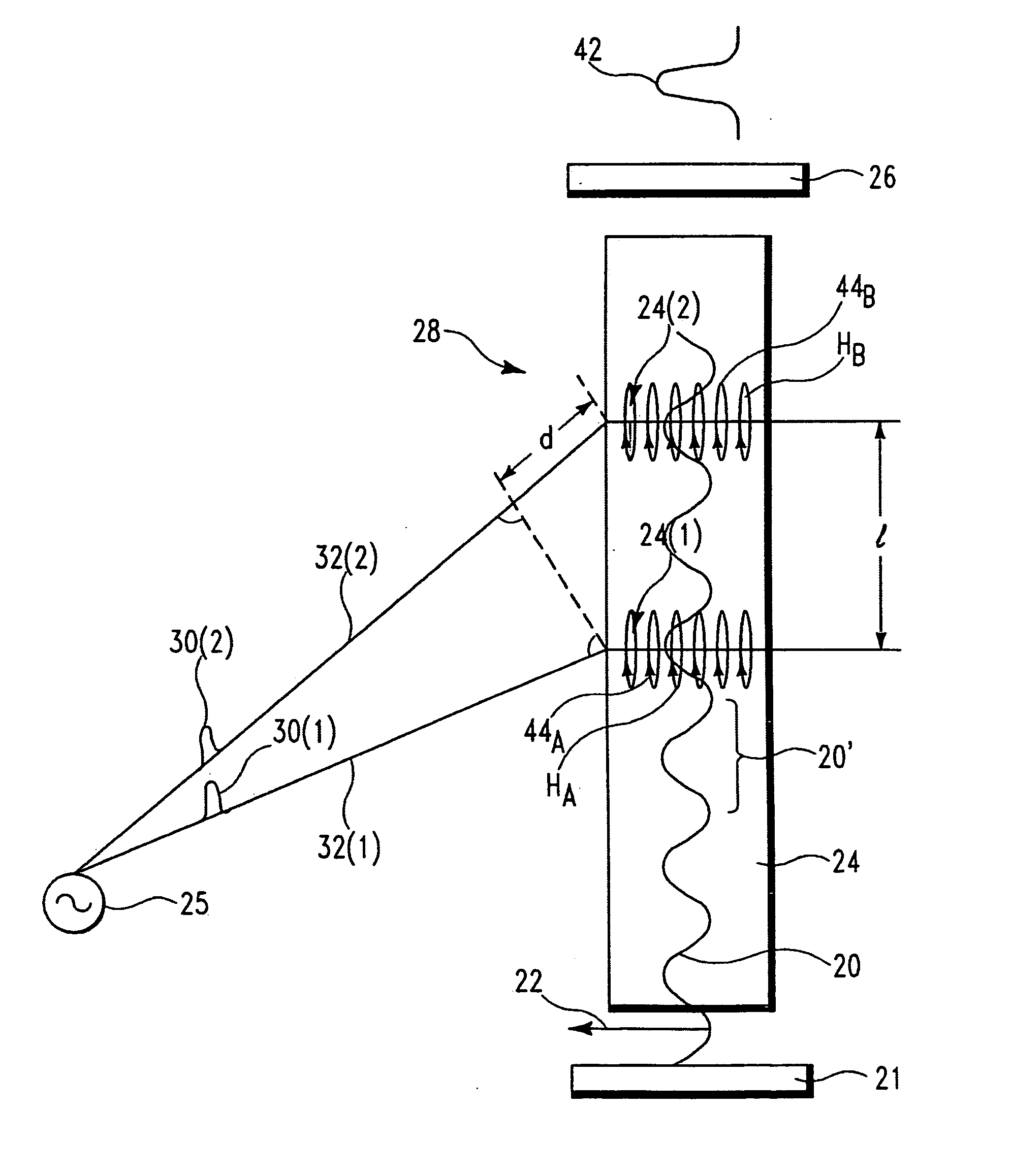
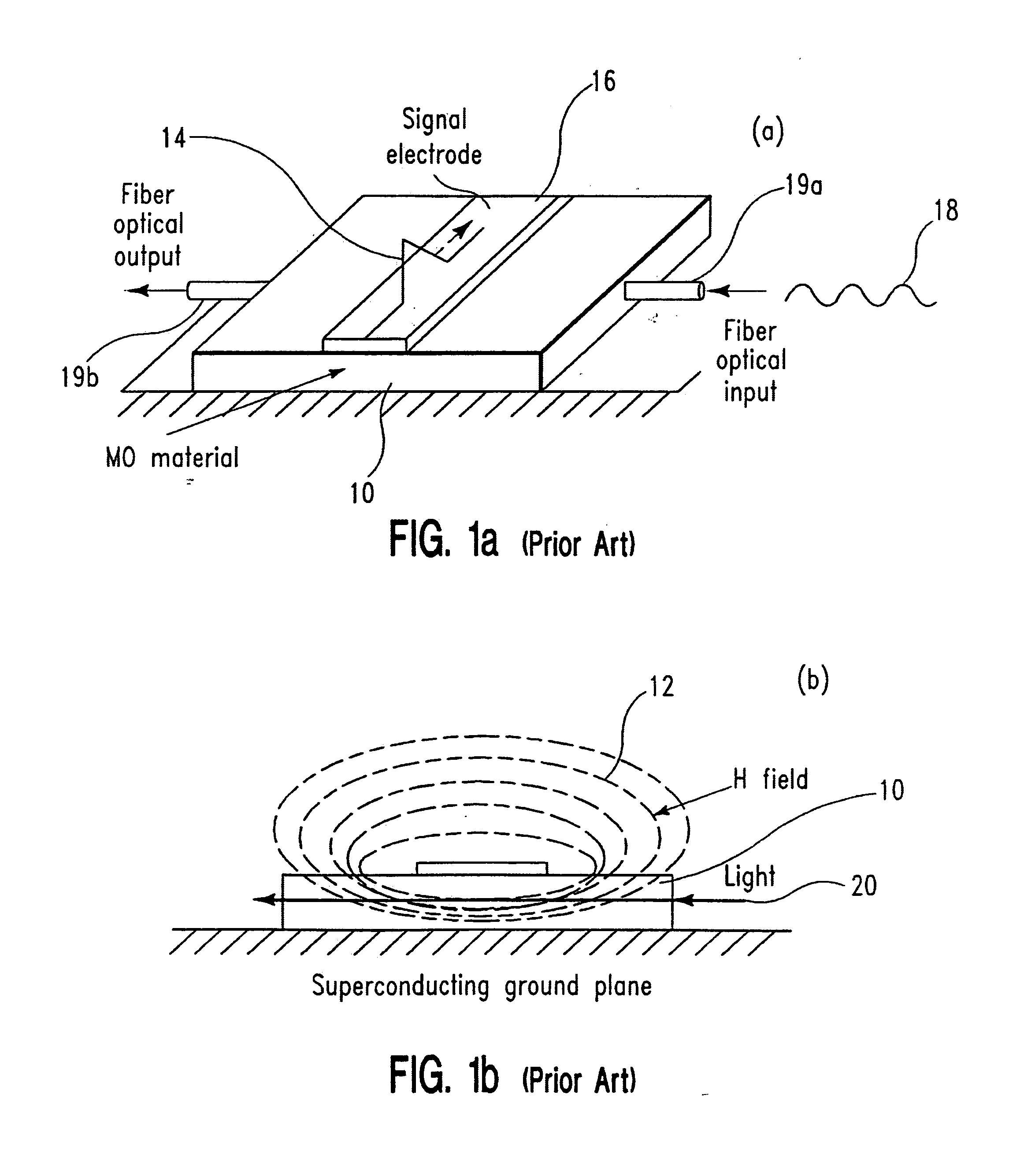
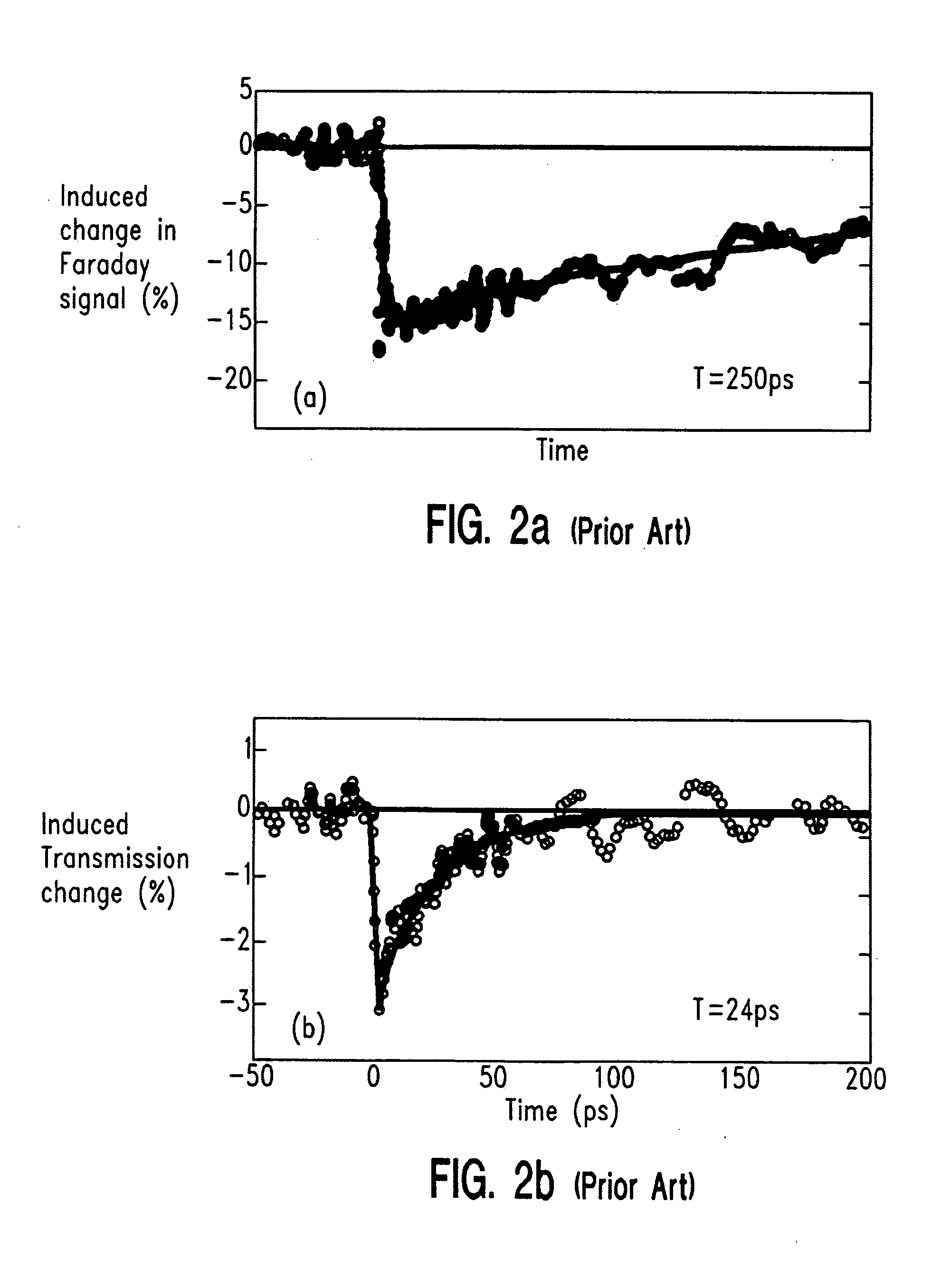
[0060] The 4.52° rotation of the polarization of light described in the Sobolewski paper for a EuSe magneto-optical waveguide was produced by a 2.51 Oe magnetic field provided by a current pulse of 1 mA flowing in a superconducting Nb-trilayer from a 10 um2 Josephson junction pulse generator. The present invention provides schemes to boost that rotation angle while increasing current pulse speed, signal amplitude, extinction coefficient, and data rate.

[0061] A review paper, “RSFQ Logic / Memory Family: A New Josephson-Junction Technology for Sub-Terahertz-Clock-Frequency Digital Systems,” by K. K. Likharev and V. K. Semenov, IEEE Transactions on Applied Superconductivity, vol. 1, No. 1, March 1991, (“the Likharev paper”), shows that the speed-performance of a Josephson junction varies inversely with the size of the junction. Extrapolating from Table 1 in the Likharev paper, the 10 um2 junction of Sobolewski would provide a switching time of 8 ps which would corresponds to a 125 GHz s...


PUM


Abstract

A short intense pulse of radiation is generated by shining radiation through a magneto-optical material and providing multiple stimulations to the material. The material is excited multiple times to rapidly change a property of the radiation, such as the angle of its polarization. The first excitation rotates the polarization in a first direction and the second excitation can rotate the polarization further. Alternatively the second excitation can bring the polarization back to its initial direction. Effect of lengthy relaxation times in the material cancel each other out and the pulse of light has a length that depends on the time difference between the two excitations and the spacing between them. This allows a pulse of light to be produced that has more rotation or has a shorter pulse width than the time for excitation plus the time for normal relaxation of the magneto-optical material.

Description

RELATED APPLICATIONS [0001] This is a divisional of U.S. patent application Ser. No. 09 / 796,025 filed Feb. 28, 2001.FIELD OF THE INVENTION [0002] This invention generally relates to optical modulation. More particularly, it relates to a device for high data rate modulation of an optical signal. Even more particularly, the invention relates to a device that provides a high amplitude and high data rate of magneto-optical modulation. BACKGROUND OF THE INVENTION [0003] Because of the high data rates available, optical fiber is preferred for high-speed transmission of data, audio, and video. Binary optical signals consist of low and high intensity signals traveling through the fiber. The limiting factor has been the speed at which light can be electrically switched or modulated to provide change from high intensity signal to low intensity signal and back to high intensity signal. This conversion from electrical to optical is slower than the capability of the fiber. While the optical fibe...

Claims


Application Information

Patent Timeline
IPC IPC(8): G02F1/09
CPCG02F2203/26G02F1/09
Inventor COTTRELL, WILLIAM J.FERENCE, THOMAS G.PUZEY, KENNETH A.
Owner COTTRELL WILLIAM J
Learn More