

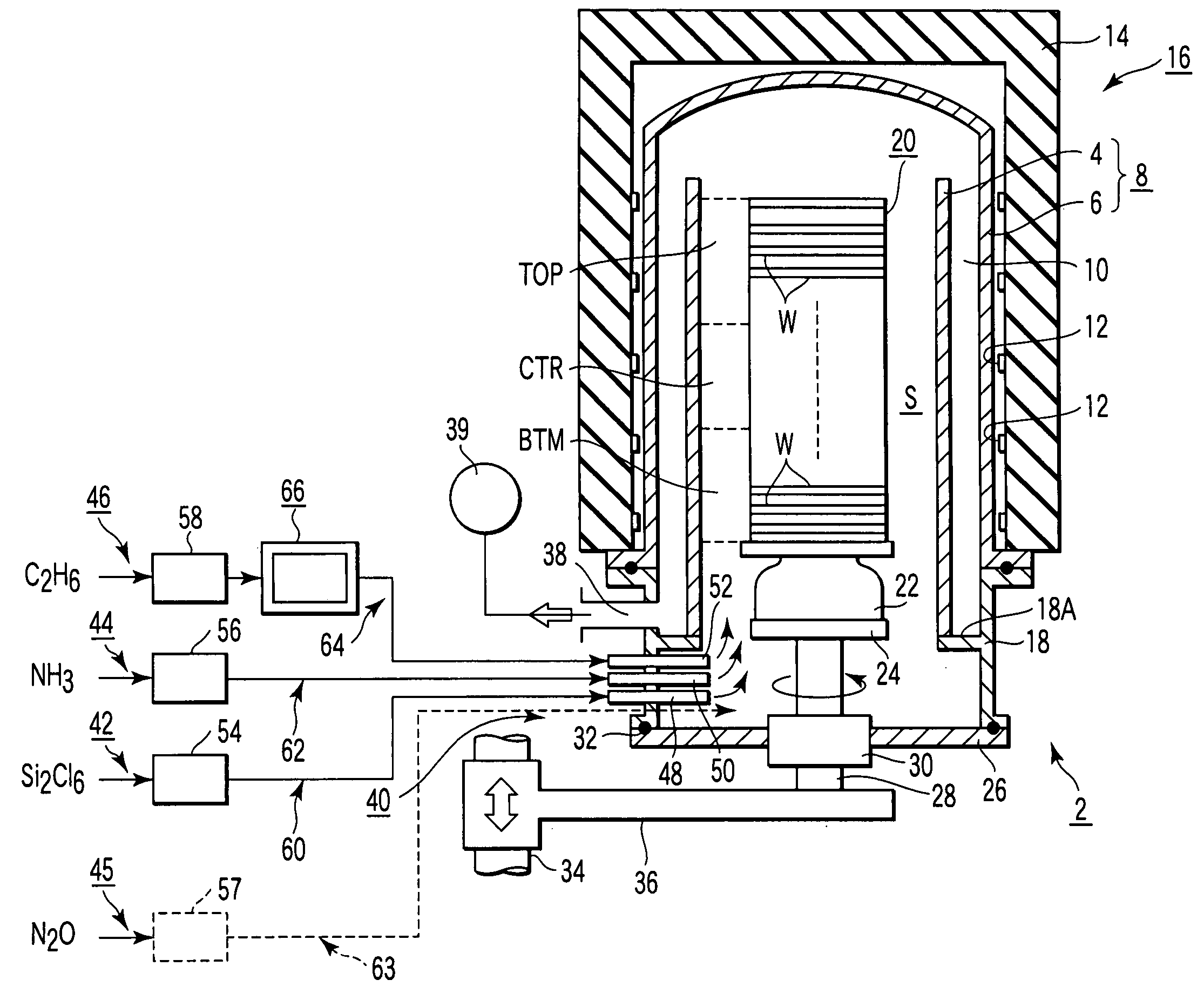
Cvd method and device for forming silicon-containing insulation film
- Summary
- Abstract
- Description
- Claims
- Application Information
AI Technical Summary
Benefits of technology
Problems solved by technology
Method used
Image

Examples
experiment 1
[Experiment 1]
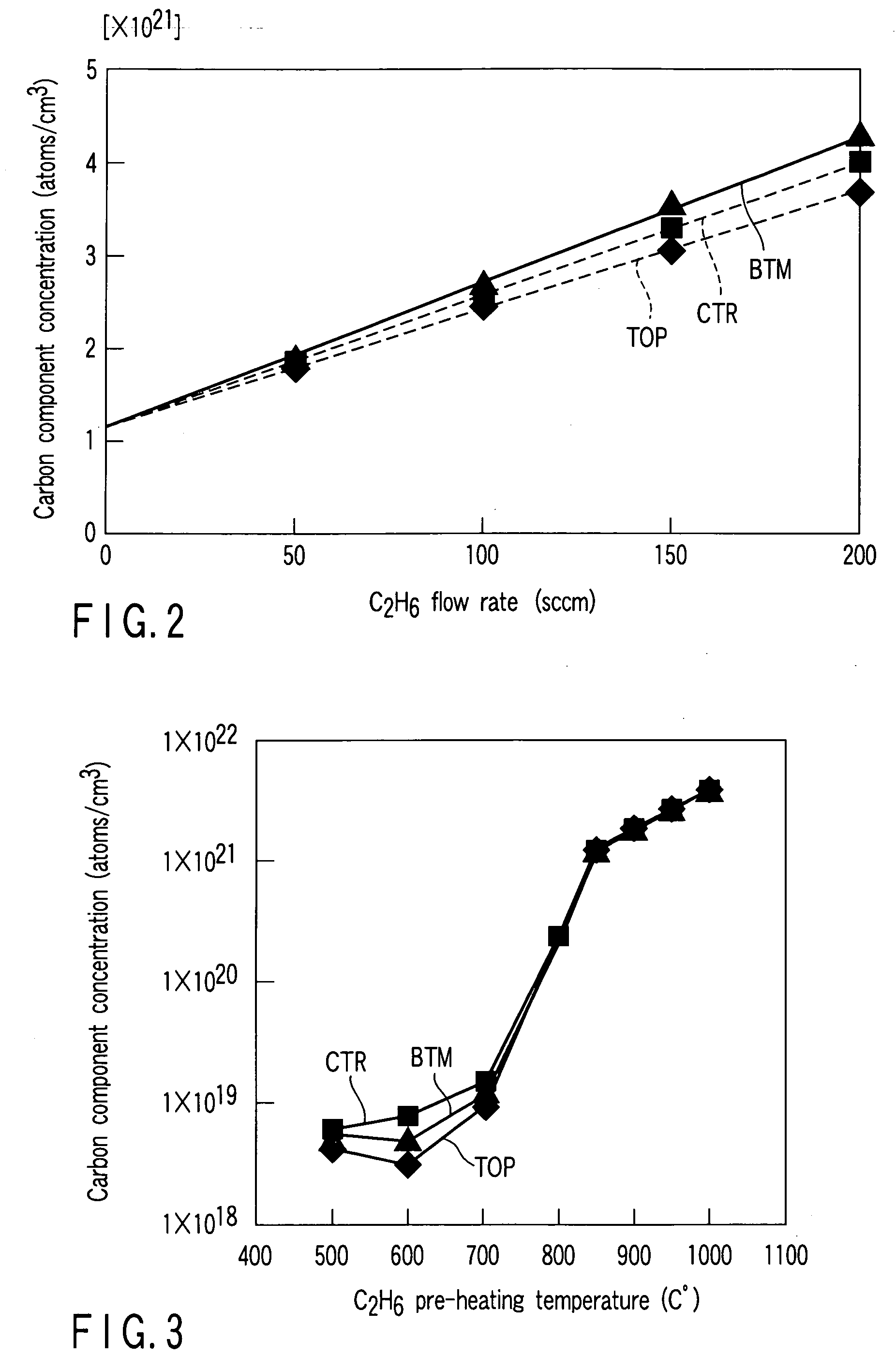
[0047] An experiment was conducted to examine the relationship between the C2H6 gas flow rate and the carbon component concentration in a silicon nitride film. This experiment employed the following conditions as constants, i.e., a process temperature of 600° C., process pressure of 27 Pa, Si2Cl6 gas flow rate of 30 sccm, NH3 gas flow rate of 900 sccm, and C2H6 gas pre-heating temperature of 1000° C. On the other hand, this experiment employed different C2H6 gas flow rates falling within a range of from 0 to 200 sccm.
[0048]FIG. 2 is a graph obtained by experiment 1 and showing the relationship between the C2H6 gas flow rate and the carbon component concentration in a silicon nitride film.
[0049] As shown in FIG. 2, the carbon component concentration in a silicon nitride film almost linearly increased with increase in the C2H6 gas flow rate within a range of from 0 to 200 sccm, without reference to the wafer positions from the top to bottom. Accordingly, it has been fo...
experiment 2
[Experiment 2]
[0050] An experiment was conducted to examine the relationship between the C2H6 gas pre-heating temperature and the carbon component concentration in a silicon nitride film. This experiment employed the following conditions as constants, i.e., a process temperature of 600° C., process pressure of 27 Pa, Si2Cl6 gas flow rate of 30 sccm, NH3 gas flow rate of 900 sccm, and C2H6 gas flow rate of 200 sccm. On the other hand, this experiment employed different C2H6 gas pre-heating temperatures within a range of from 500 to 1000° C.
[0051]FIG. 3 is a graph obtained by experiment 2 and showing the relationship between the C2H6 gas pre-heating temperature and the carbon component concentration in a silicon nitride film.
[0052] As shown in FIG. 3, where the C2H6 gas pre-heating temperature was within a range of from 500 to 700° C., the carbon content concentration in a silicon nitride film gradually increased in principle, although there was a partly downward trend, which seems ...
experiment 3
[Experiment 3]
[0054] With reference to the results of experiments 1 and 2, an experiment was conducted to examine the relationship between the carbon component concentration in a silicon nitride film and the etching rate thereof relative to dilute hydrofluoric acid. This experiment employed the following conditions as constants, i.e., a process temperature of 600° C., process pressure of 27 Pa, Si2Cl6 gas flow rate of 30 sccm, NH3 gas flow rate of 900 sccm, and C2H6 gas flow rate of 200 sccm. On the other hand, this experiment employed different pre-heating temperatures to vary the carbon component concentration in a silicon nitride film within a range of from 1×10¹⁸ to 1×10²² atms / cm3.
[0055]FIG. 4 is a graph obtained by experiment 3 and showing the relationship between the carbon component concentration in a silicon nitride film and the normalized etching rate thereof relative to dilute hydrofluoric acid (49%-HF:H2O=1:100).
[0056] A shown in FIG. 4, the etching rate linearly decre...
PUM
| Property | Measurement | Unit |
|---|---|---|
| Temperature | aaaaa | aaaaa |
| Temperature | aaaaa | aaaaa |
| Temperature | aaaaa | aaaaa |
Abstract
Description
Claims
Application Information