Semiconductor memory devices and methods of fabricating semiconductor memory device
a memory device and semiconductor technology, applied in semiconductor devices, digital storage, instruments, etc., can solve the problems of increasing the cost of storage, reducing the amount of spontaneous polarization of ferroelectric capacitors, and affecting the data retention rate, so as to improve the data retention rate and charge retention capacity , the effect of improving the data retention rate in a high temperature environmen
- Summary
- Abstract
- Description
- Claims
- Application Information
AI Technical Summary
Benefits of technology
Problems solved by technology
Method used
Image


Examples
first embodiment
(1) First Embodiment
[0028] (Configuration)
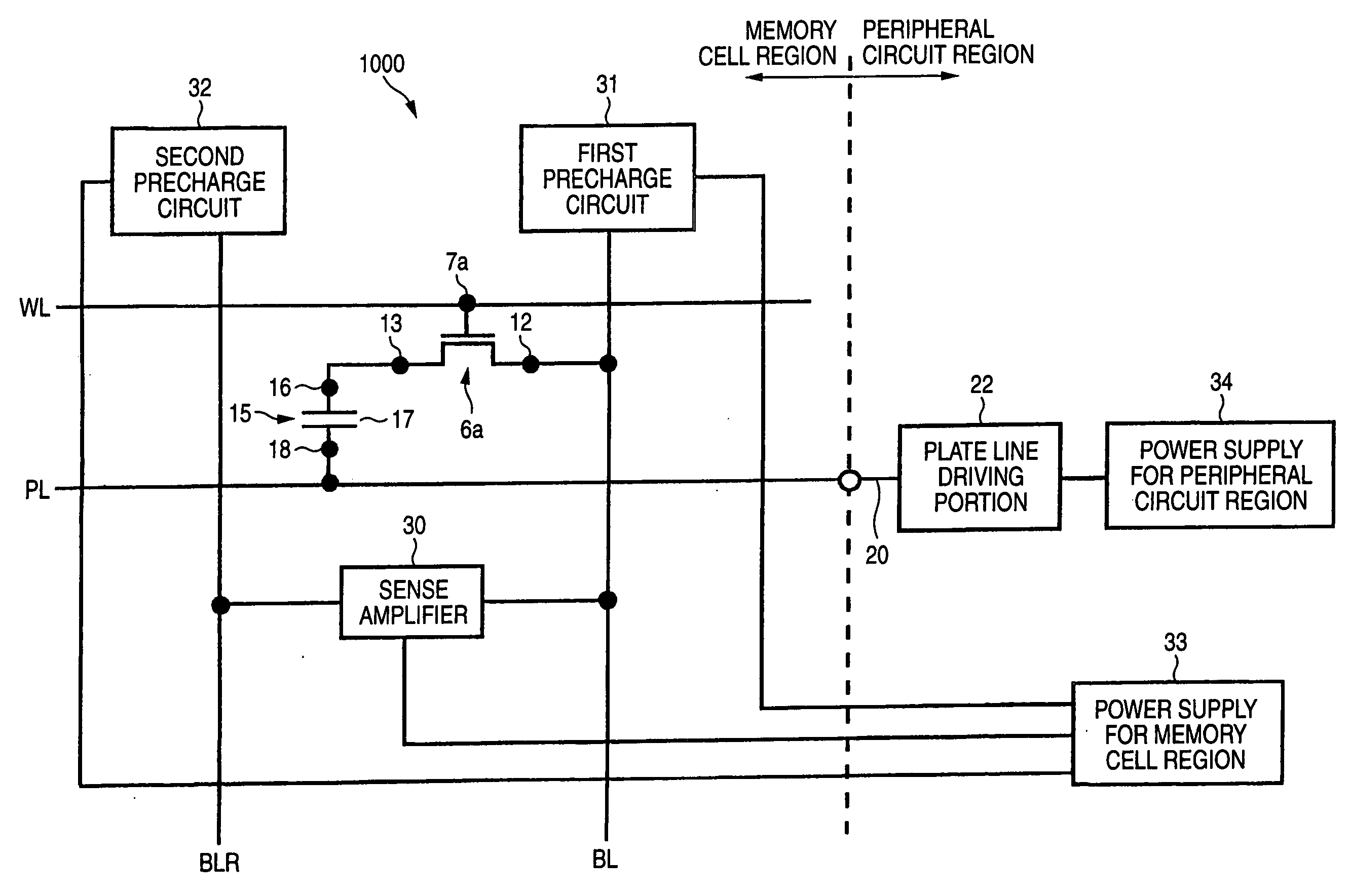
[0029]FIG. 1 is an electric circuit diagram of a semiconductor memory device 1000 involving a first embodiment of the invention. FIG. 3D is a sectional diagram of the semiconductor memory device 1000. The semiconductor memory device 1000 is applied to a non-volatile memory device that makes use of a ferroelectric capacitor. The semiconductor memory device 1000 includes a memory cell region (first semiconductor region) and a peripheral circuit region (second semiconductor region).
[0030] In the memory cell region, a word line WL, a bit line BL, a reference bit line BLR, a plate line PL, at least one memory cell, a sense amplifier 30, a first precharge circuit 31 and a second precharge circuit 32 are formed. The memory cell region, as mentioned below, is formed on an SOI substrate (Silicon On Insulator) made of a supporting substrate 1 that is a semiconductor substrate, an insulating film 2 formed on a surface of the supporting substrate 1, a...
second embodiment
(2) Second Embodiment
[0073] (Configuration)
[0074]FIG. 10 is a sectional diagram of a semiconductor memory device 1000b involving a second embodiment. An electric circuit diagram of the semiconductor memory device 1000b is the same as FIG. 1.
[0075] In the present embodiment, in a memory cell region, an active region 4a of a selection transistor 6a is formed on a supporting substrate 1 that is a substrate bulk region. On the other hand, a control transistor 6b, similarly to the case of the first embodiment, is formed on a semiconductor film 4. Furthermore, similarly to FIG. 1, a power supply for memory cell region 33 and a power supply for peripheral circuit region 34 are formed in separate systems and completely insulated at the time of non-operation. Still furthermore, a ground line GND1 and a ground line GND2 are insulated from each other.
[0076] (Method of Fabrication)
[0077] In the following, a method of fabricating the semiconductor memory device 1000b will be explained with r...
third embodiment
[0087] (Configuration)
[0088]FIG. 12 is a sectional diagram of a semiconductor memory device 1000c involving a third embodiment. An electric circuit diagram of the semiconductor memory device 1000c is the same as FIG. 1.
[0089] In the present embodiment, an active region 4a of a selection transistor 6a is, similarly to the first embodiment, formed through an insulating film 2 on a supporting substrate 1. On the other hand, active regions of transistors in the peripheral circuit region such as an active region 4b of a control transistor 6b and so on are formed on the supporting substrate 1 that is a substrate bulk region. Furthermore, similarly to FIG. 1, a power supply for memory cell region 33 and a power supply for peripheral circuit region 34 are formed into separate systems and completely insulated at the time of non-operation. Still furthermore, a ground line GND1 and a ground line GND2 are insulated from each other.
[0090] (Method of Fabrication)
[0091] In the following, a met...
PUM
 Abstract
Description
Claims
Application Information
PatSnap Eureka turns technology decisions into work you can execute. Powered by our Innovation Knowledge Graph, it runs expert workflows across engineering, life sciences, materials and intellectual property. Get your review-ready output in minutes.


