A/d conversion processing apparatus providing improved elimination of effects of noise through digital processing, method of utilizing the a/d conversion processing apparatus, and electronic control apparatus incorporating the a/d conversion processing apparatus
- Summary
- Abstract
- Description
- Claims
- Application Information
AI Technical Summary
Benefits of technology
Problems solved by technology
Method used
Image
Examples
first embodiment
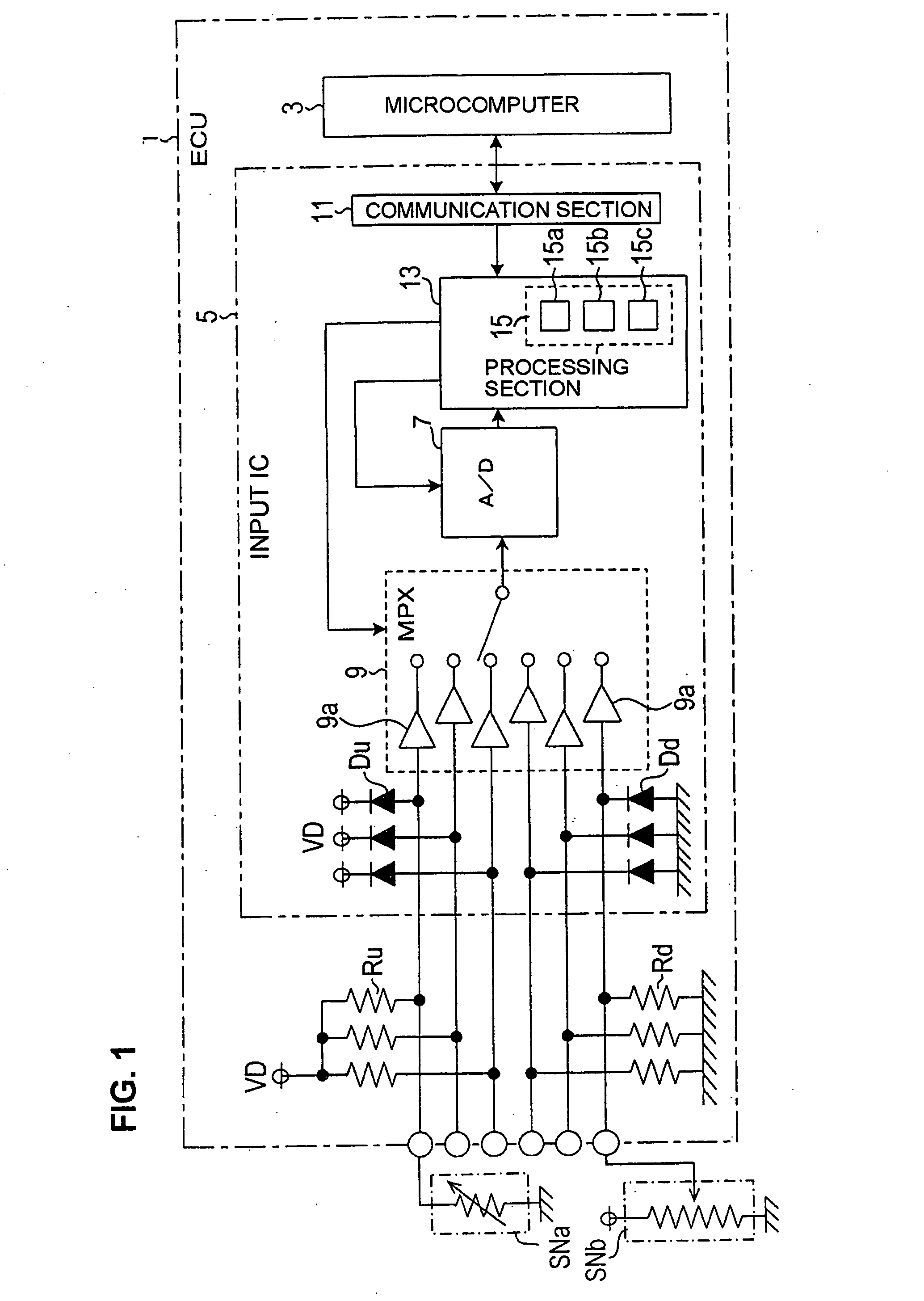
[0080]FIG. 1 is a system block diagram of a first embodiment, in which an ECU 1 is made up of a microcomputer 3 that controls a vehicle engine and an input IC 5 for performing A / D conversion of a plurality of input analog signals (in this embodiment, 6 signals). These analog signals are produced by respective sensors which detect various operating parameters of the engine. Digital signals respectively corresponding to the input analog signals are supplied from the input IC 5 to the microcomputer 3, e.g., multiplexed as successive sets of digital values, for use in performing the control operations.
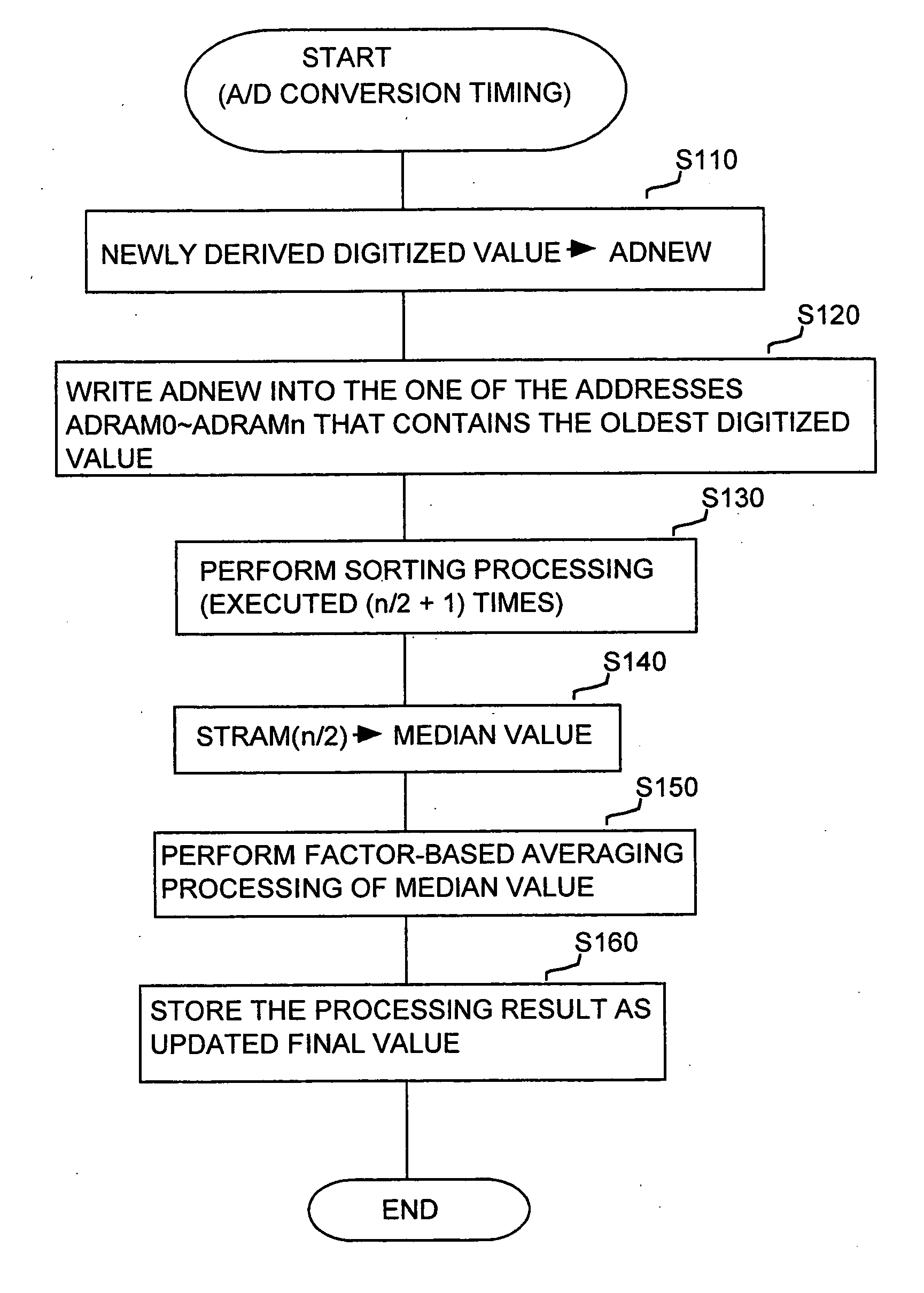
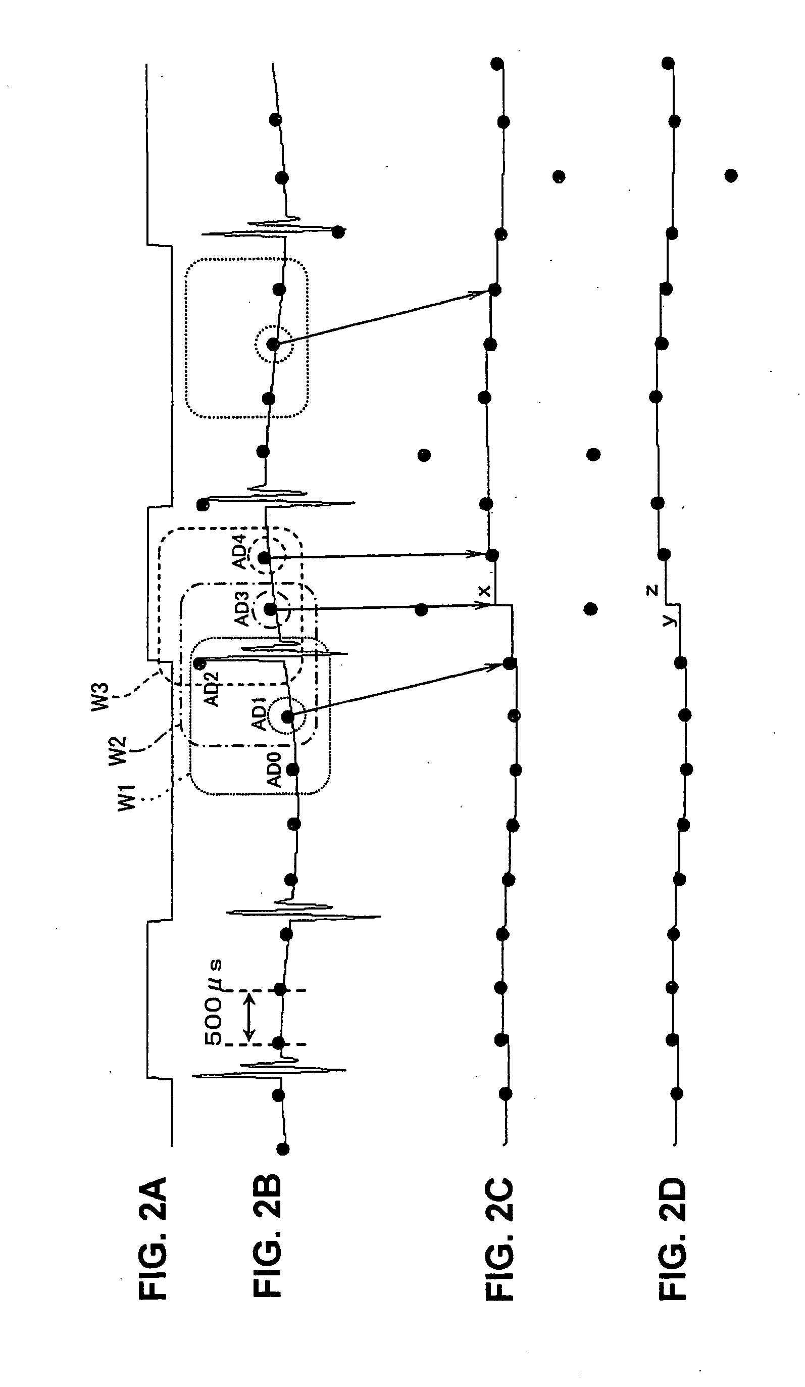
[0081] The input IC 5 includes an A / D converter 7, a multiplexer 9 which cyclically selects the input analog signals, to supply these to the A / D converter 7, a communication section 11 for performing serial data communication with the microcomputer 3, and a processing section 13 which controls the multiplexer 9 and the A / D converter 7 and processes the A / D converted values that are produc...
second embodiment
[0123] A second embodiment of an ECU will be described in the following. Since the hardware configuration of this embodiment can be identical to that of the first embodiment, only points of difference between the ECUs of the first and second embodiments will be described in detail, and components of the second embodiment having functions corresponding to those of the first embodiment will be designated by corresponding reference numerals to those of the first embodiment. The above is also true of other embodiments described hereinafter, unless otherwise indicated.
[0124] It will further be assumed that with the second embodiment, the interval between successive A / D conversions of an input analog signal is 250 μs and the value of n is 4. In the same way as for the first embodiment, only the processing applied to a single input analog signal will be described, unless otherwise indicated.
[0125]FIGS. 9A, 9B, 9C are a timing diagrams for use in describing the operation of the second emb...
third embodiment
[0131] A third embodiment will be described in the following. In the same way as for the preceding embodiments, the description will be based on processing of a single input analog signal. The ECU 1 of this embodiment differs from that of the first embodiment in that the sorting processing-use memory region 15b of the RAM 15 is omitted. Furthermore, instead of the processing of FIG. 4 described above, the processing sequence shown in FIG. 10 is executed by the processing section 13 of the input IC 5 of the third embodiment each time an A / D conversion has been performed. However the processing of FIG. 10 does not begin to be executed until after a total of (n+1) A / D conversion operations of the corresponding analog signal have been completed following switch-on of power to operate the ECU 1 and the start of operation (where n is an even-numbered integer, of value 2 or greater).
[0132] Specifically, following the start of operation of the ECU 1, when a total of (n+1) digital values re...
PUM
 Abstract
Description
Claims
Application Information


