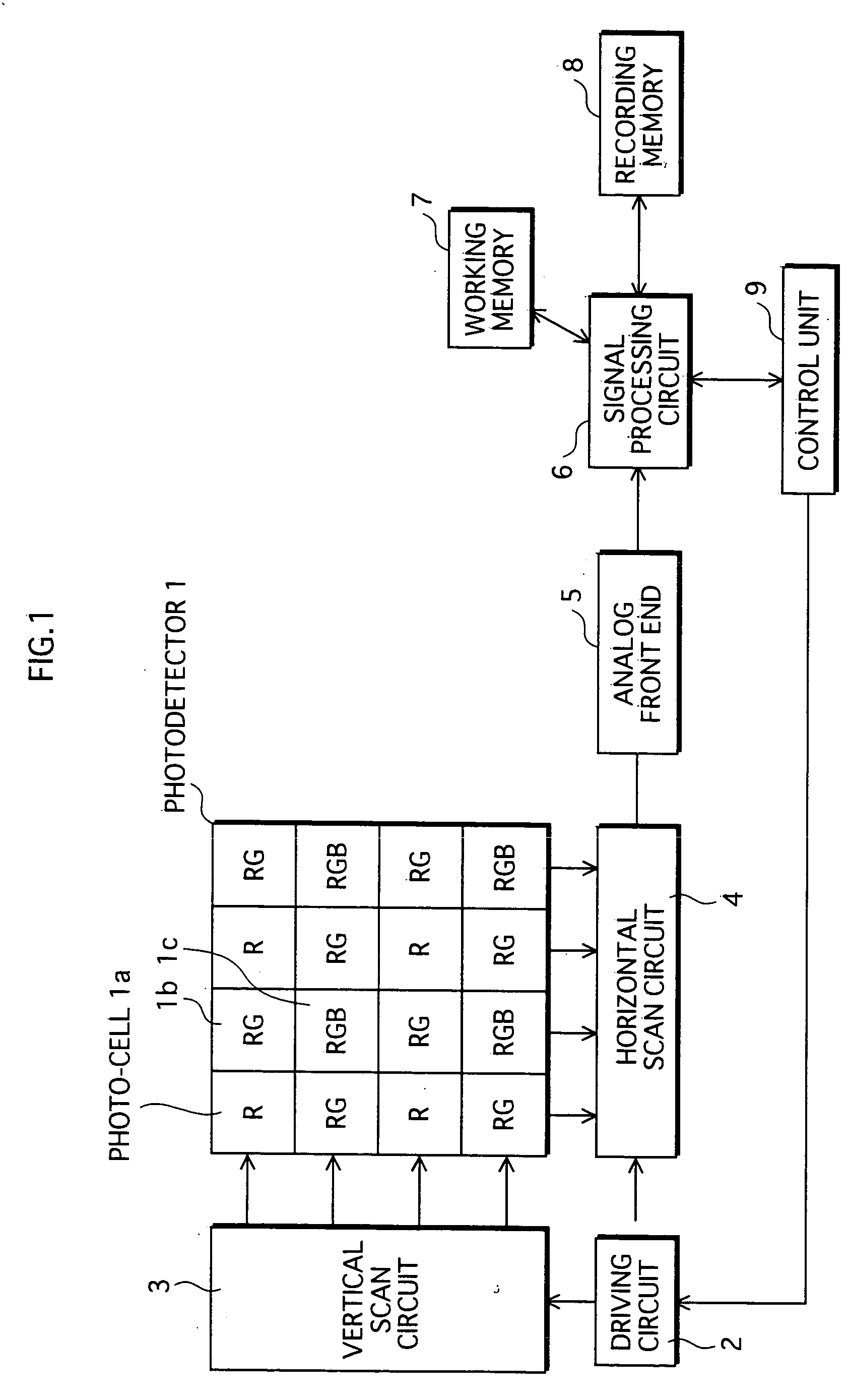
Photodetector

a technology of photodetectors and detectors, applied in the field of photodetectors, can solve the problems of reducing the cost of photodetectors, and achieve the effect of simplifying the manufacturing process

Active Publication Date: 2005-05-19
PANASONIC CORP
View PDF5 Cites 99 Cited by
  • Summary
  • Abstract
  • Description
  • Claims
  • Application Information

AI Technical Summary

Benefits of technology

[0060] Further, the filter layers can be manufactured using a semiconductor fabrication technology. Therefore, a color filter manufacturing process that manages acrylic resins is not necessary. As a result, it is possible to utilize manufacturing facilities for semiconductor fabrication as well as to simplify the manufacturing process.

Problems solved by technology

Manufacturing the conventional color filters, however, requires a troublesome material management for the pigments or dyestuff of different colors in the manufacturing process, and this hinders the cost reduction of the photodetectors.

Method used


Image

  • Photodetector
  • Photodetector
  • Photodetector

Examples


first embodiment

[outline]

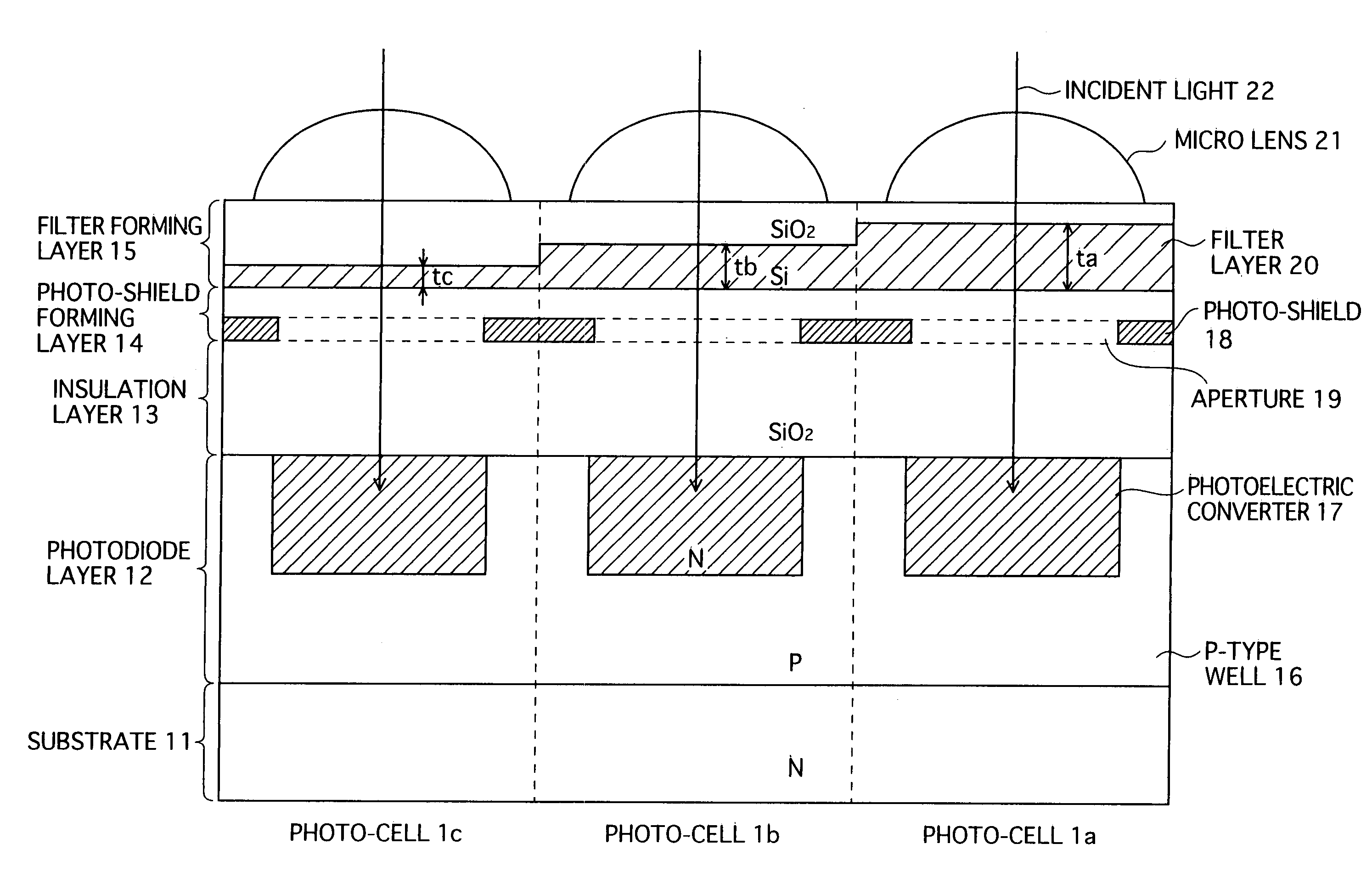
[0076] In a first embodiment, filter layers in all pixel cells are made only of polysilicon. As a characteristic of polysilicon, a wavelength range of light to be transmitted through a polysilicon layer varies according to the thickness of the layer. Therefore, it is possible to use the polysilicon filter layers as color filters by setting a thickness of polysilicon for each photo-cell is different from cell to cell.

[0077] Because the wavelength range of light to be transmitted through a polysilicon filter layer is determined based on the thickness of the corresponding filter layer, instead of pigments or dyestuff for each color, it is not necessary to control material for the pigments or dyestuff of different colors in manufacturing the filter layers. Therefore, the production cost can be reduced.

[0078] In addition, the filter layers can be manufactured using a semiconductor fabrication technology, and a color filter manufacturing process that manages acrylic resins is ...

second embodiment

[Outline]

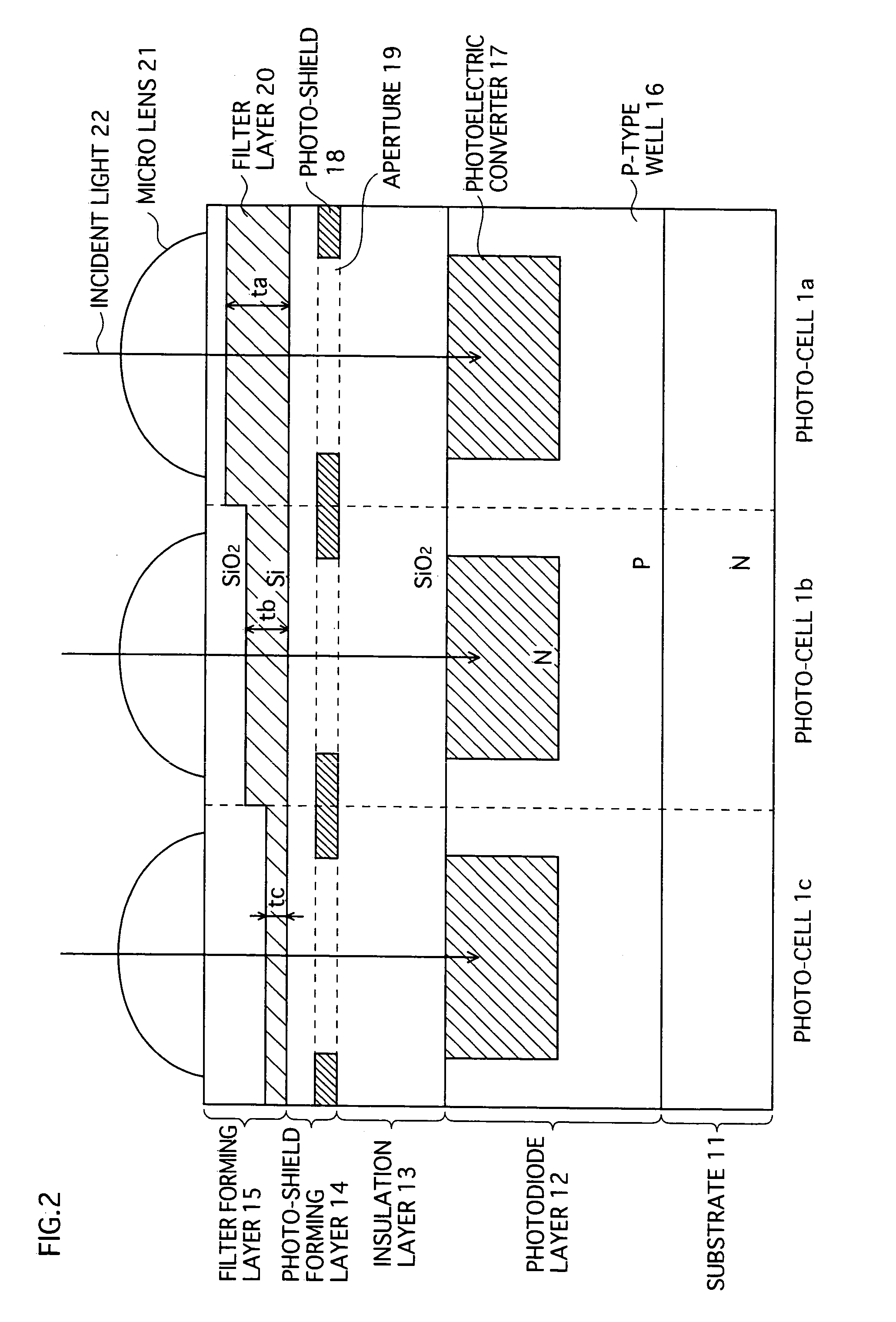
[0156] In a second embodiment, the filter forming layer 15 is formed below the photo-shield forming layer 14, and the insulation layer 13 that insulates between the filter forming layer 15 and the photodiode layer 12 is formed so as to have a thickness in a range of 1 nm to 150 nm. With photo-cells having such a structure, reflections of the incident light 22 at boundaries between layers become smaller, and as a result, it is possible to suppress a decrease in sensitivity.

[Structure]

[0157] FIG.7 is a sectional view of photo-cells (1a, 1b, 1c) according to the second embodiment.

[0158] The photo-cells according to the second embodiment each include the substrate 11, the photodiode layer 12, the insulation layer 13, the photo-shield forming layer 14, and the filter forming layer 15. A difference from the photo-cells according to the first embodiment is that the filter forming layer 15 is formed between the photo-shield forming layer 14 and the insulation layer 13. Other th...

third embodiment

[Outline]

[0171] In a third embodiment, the insulation layer 13 between the filter layer 20 and the photodiode layer 12 is removed from the photo-cells in order to improve the sensitivity of the photo-cells. However, simply removing the insulation layer 13 causes another problem that the signal charge generated in the photoelectric converter 17 leak to the filter layer 20. Therefore, a potential barrier 23 is disposed between the photoelectric converter 17 and the filter layer 20 so as to prevent the signal charges from leaking. By this, it is possible to completely eliminate the reflection at the boundary between the insulation layer 13 and the photodiode layer 12.

[Structure]

[0172] FIG.8 is a sectional view of photo-cells (1a, 1b, 1c) according to a third embodiment.

[0173] The photo-cells each include the substrate 11, the photodiode layer 12, the photo-shield forming layer 14, and the filter forming layer 15. A difference from the photo-cells according to the second embodiment ...


PUM


Abstract

A photodetector includes a semiconductor substrate having photo-cells (1a, 1b, 1c). Each photo-cell is provided with a filter layer 20 that transmits light in a wavelength range predetermined for the photo-cell, and a photoelectric converter 17 that generates a signal charge according to an intensity of the light transmitted through the filter layer 20. Thickness (ta, tb, tc) of the filter layers 20 are corresponding to the wavelength ranges predetermined for respective photo-cells. By such a structure, it is possible to provide cost effective photodetectors that can be manufactured without managing materials for pigments and dyestuff for different colors when making color filters.

Description

BACKGROUND OF THE INVENTION [0001] (1) Field of the Invention [0002] The present invention relates to photodetectors such as image sensors, and more specifically to color filters provided to photo-cells in a photodetector. [0003] (2) Description of the Related Art [0004] A commonly used photodetector includes a semiconductor substrate having a plurality of photo-cells, and each photo-cell is provided with a color filter and a photodiode. There are red color filters (R), green color filters (G), and blue color filters (B) in one photodetector, and each photo-cell is assigned with a color filter having one of the three colors. The photodiodes generate signal charges responsive to the intensity of the light that has passed through the color filters. Consequently, a signal charge for light of a specific color in the incident light is generated in each photo-cell. Imaging data for one picture is generated by collecting the signal charges for the three colors generated in the photo-cells ...

Claims


Application Information

Patent Timeline
Patent Type & Authority Applications(United States)
IPC IPC(8): G01J1/02H01L27/14H01L27/146H01L31/00H01L31/0232
CPCH01L27/14621H01L27/14623H01L31/0232H01L27/14685H01L27/14627H01L31/02327
Inventor YAMAGUCHI, TAKUMIKASUGA, SHIGETAKAMURATA, TAKAHIKO
Owner PANASONIC CORP
Why Eureka
Try Eureka