Light emitting device and electric device using the same

a technology of light emitting devices and electric devices, applied in static indicating devices, organic semiconductor devices, instruments, etc., can solve problems such as hard to generate noise, deterioration of luminance, and major problems of reliability of devices, and achieve the effect of improving conductivity

Inactive Publication Date: 2005-05-19
SEMICON ENERGY LAB CO LTD
View PDF19 Cites 24 Cited by
  • Summary
  • Abstract
  • Description
  • Claims
  • Application Information

AI Technical Summary

Benefits of technology

[0032] Besides, the invention is characterized in that a layer containing a conductive polymer compound is disposed between the organic compound layer and the first electrode, or between the organic compound layer and the second electrode. Particularly, in view of improving

Problems solved by technology

Further, since the organic light emitting device is a carrier-injecting type light emitting device, it can be driven by DC voltage, and is hard to generate noise.
However, the reliability of the device can be a major problem of such a light emitting device.
With respect to the reliability, the luminance being deteriorated over time is a particularly conspicuous problem, and a considerable improvement is needed.
However, when the luminance is being reduced over time, the current efficiency (the ratio of the lum

Method used


Image

  • Light emitting device and electric device using the same
  • Light emitting device and electric device using the same
  • Light emitting device and electric device using the same

Examples


embodiments

Embodiment 1

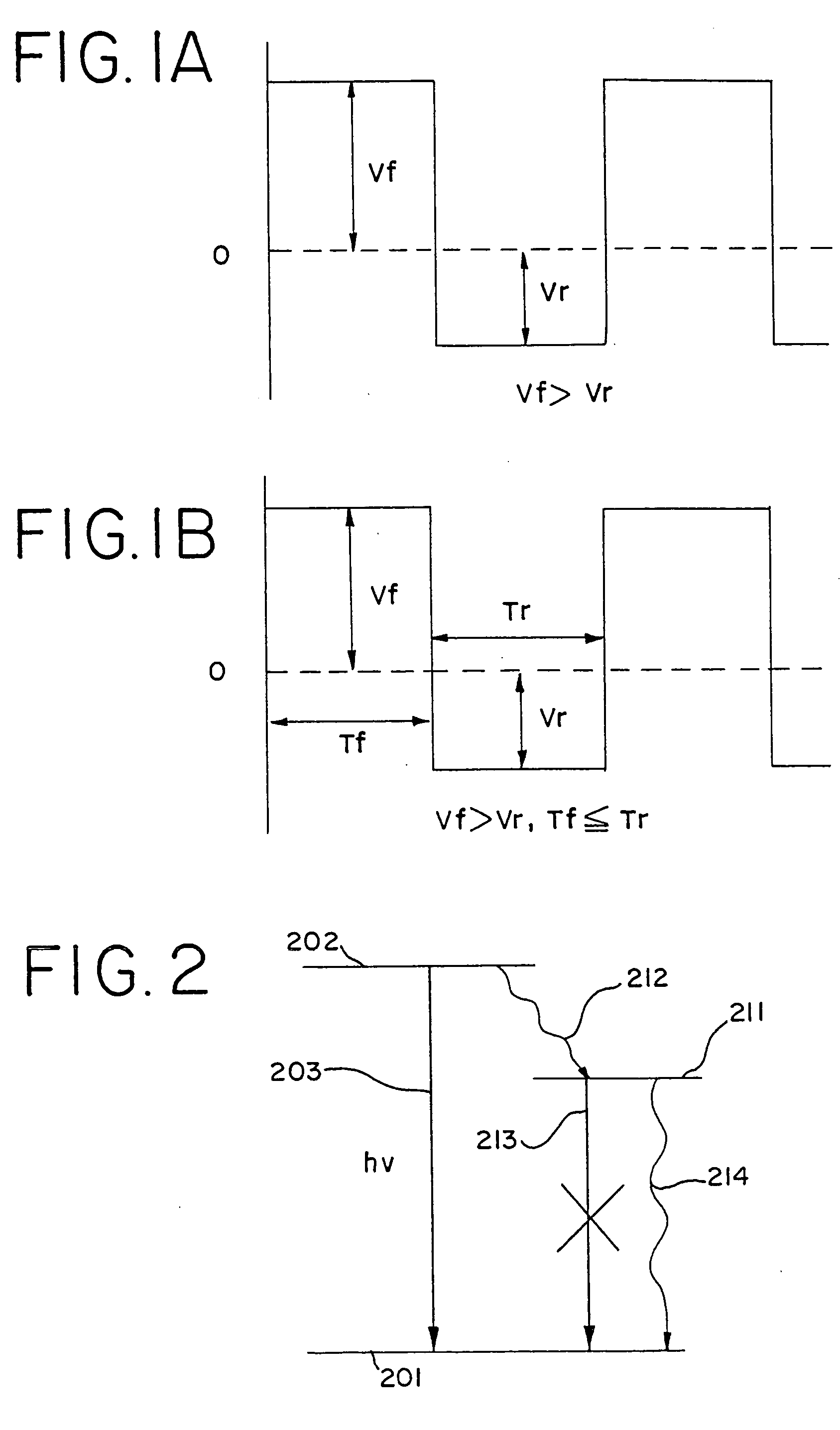
[0073] In the embodiment, in a organic light emitting element in which a polymer compound producing light emission was applied as an organic compound layer and a layer including a conductive polymer compound was disposed between an anode and the organic compound layer, luminance deterioration was measured in the constant voltage alternating current drive (the drive in which both the forward bias and the reverse bias are set to a fixed voltage).

[0074]FIG. 5 shows a device structure. First, an aqueous solution of 1.3 wt % of PEDOT / PSS was applied to a glass substrate 501 deposited with ITO of a thickness of 110 nm as an anode 502, and the substrate was baked at a temperature of 100° C. for one hour to form a layer 503 containing a conductive polymer compound. The film thickness was formed to be about 30 nm.

[0075] Subsequently, the substrate was vacuum-baked at a temperature of 80° C. for three minutes, and a toluene solution of 0.16 g of poly(p-phenylene vinylene) deriva...

embodiment 2

[0080] In this embodiment, the same device as Embodiment 1 was fabricated, and the reliability of the device was measured as the driving conditions were slightly varied. The constant voltage alternating current drive was performed where a forward bias was 3.8 [V], a reverse bias was 1.4 [V], a duty ratio was 50%, and a frequency was 600 Hz (the initial luminance at this time was about 300 cd / cm2). The result is shown by Plot AC in FIG. 7. About 60% of the initial luminance was maintained even after about 700 hours passed.

embodiment 3

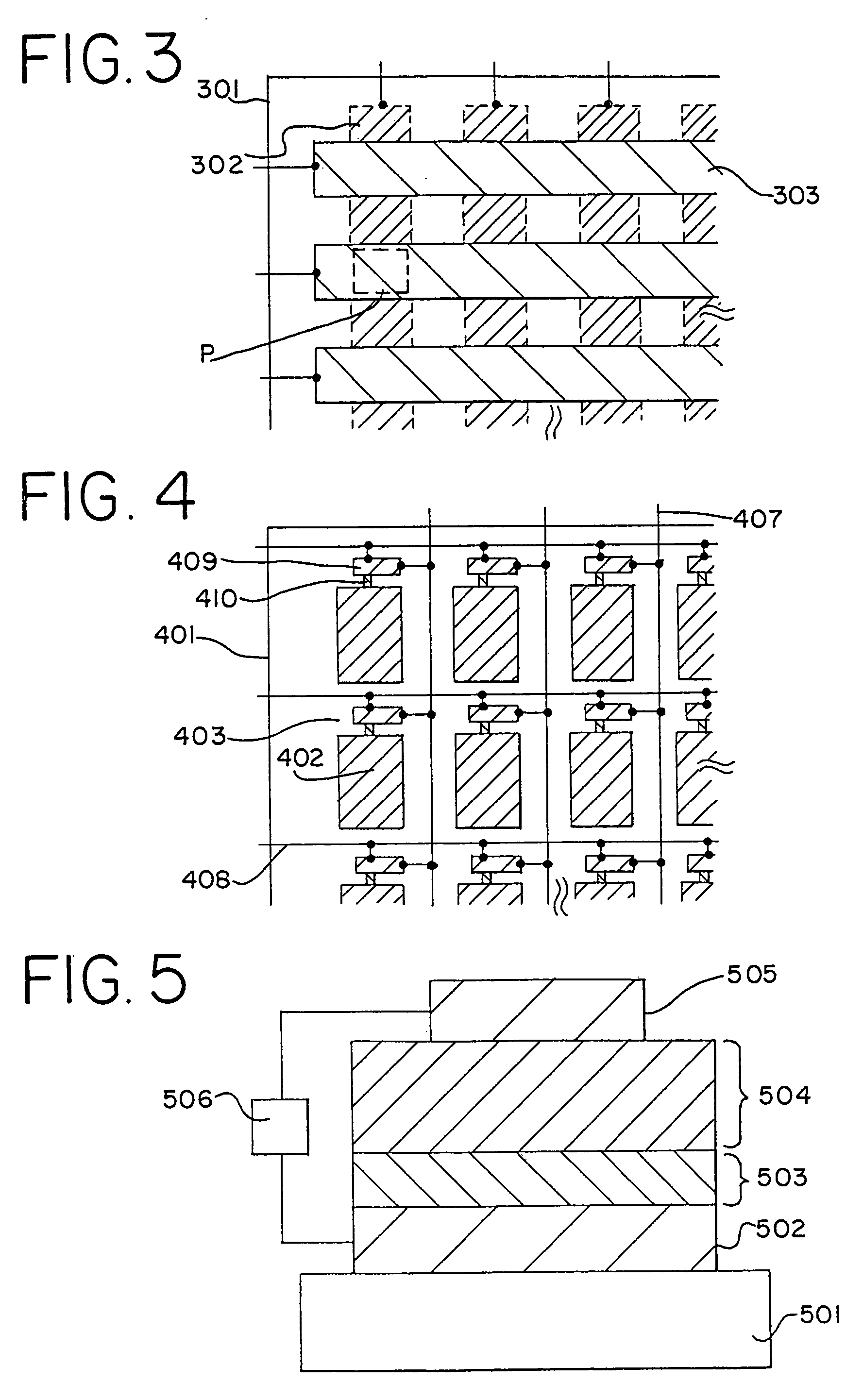
[0083] An example of a passive matrix light emitting device is shown in Embodiment 3 as an example of a light emitting device disclosed by the present invention. A top view thereof is shown in FIG. 8A, and a cross sectional diagram of FIG. 8A cut along a line P-P′ is shown in FIG. 8B. In addition, element structures of the organic light emitting element can be various, the compositions such as ones shown in Embodiments 2 and 3 may be adapted.

[0084] Reference numeral 801 denotes a substrate in FIG. 8A, and glass is used for the substrate here. A plastic material also can be used; as the plastic material, polyimide, polyamide, acrylic resin, epoxy resin, PES (polyether sulfile), PC (polycarbonate), PET (polyethylene terephthalate), or PEN (polyethylene naphthalate), which are in a plate shape, or a film shape can be used.

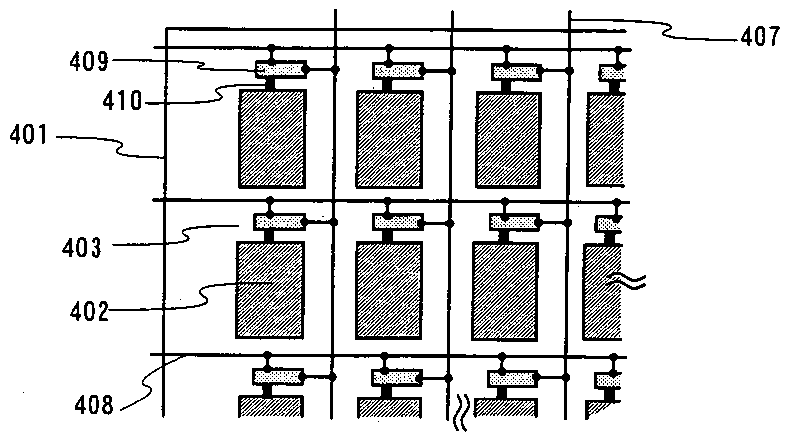
[0085] Reference numeral 802 denotes a scanning line (anode) made from an oxide conductive film, and an indium tin oxide (ITO) is used in Embodiment 3. Further, ref...


PUM


Abstract

The purpose of the present invention is to provide a light emitting device using an organic light emitting element and allowed to be driven stably with long lifetime. In a light emitting device having an organic light emitting device provided with an organic compound layer for obtaining light emission by applying a voltage between a first electrode and a second electrode, and means for applying a forward bias for emitting light from the organic light emitting device and a reverse bias of reverse polarity to the forward bias, the maximum voltage Vf of the forward bias is higher than the maximum voltage Vr of the reverse bias in an alternating current cycle formed of the forward bias and the reverse bias. At this time, the Vr is preferably a quarter of the Vf or higher than that. Additionally, the time Tr to apply the reverse bias in the alternating current cycle is preferably equal to or longer than the time Tf to apply the forward bias.

Description

BACKGROUND OF THE INVENTION [0001] 1. Filed of the Invention [0002] The present invention relates to an organic light emitting device having an anode, a cathode, and a layer containing organic compounds in which luminescence can be obtained by applying an electronic field (hereafter referred to as organic compound layer). The present invention particularly relates to an organic light emitting element having a longer drive life than that of conventional ones, and a light emitting device using the organic light emitting element. [0003] 2. Description of the Related Art [0004] An organic light emitting element is an element which emits light when an electronic field is applied. A luminescence mechanism thereof has been said: applying a voltage to an organic compound layer interposed between electrodes, electrons injected from a cathode and positive holes injected from an anode recombine together at a center of luminescence in the organic compound layer to form excited molecules; energy...

Claims


Application Information

Patent Timeline
IPC IPC(8): H05B44/00
CPCG09G3/3216G09G3/3225H05B33/0896G09G2320/043H01L2251/564G09G2310/0256H05B45/60Y02B20/30H10K71/841
Inventor SEO, SATOSHINAKASHIMA, HARUEYAMAZAKI, SHUNPEI
Owner SEMICON ENERGY LAB CO LTD
Why Eureka
Try Eureka