Surface wave excitation plasma CVD system

a surface wave excitation and plasma technology, applied in the field of cvd systems, can solve the problems of being restricted, undetected, rather, and achieve the effect of incredible high film deposition rate in the vicinity of the dielectric pla

Inactive Publication Date: 2005-05-26
SHIMADZU CORP
View PDF21 Cites 118 Cited by
  • Summary
  • Abstract
  • Description
  • Claims
  • Application Information

AI Technical Summary

Benefits of technology

[0006] Since the plasma density is high in the vicinity of the dielectric plate which generates a SWP, with a prior art system as described above in which the material gas is fed in the vicinity of the dielectric plate, the chemical reactions in this region proceed very violently. Due to this, the film deposition rate in the vicinity of the dielectric plate is incredible high; but the film deposition rate becomes exponentially l

Problems solved by technology

In other words, there is the problem that, even in the plasma area, the area in which it is possible to deposit a film which is appropri

Method used


Image

  • Surface wave excitation plasma CVD system
  • Surface wave excitation plasma CVD system
  • Surface wave excitation plasma CVD system

Examples


Embodiment Construction

[0024] In the following, preferred embodiments of the surface wave excitation plasma CVD system according to the present invention (hereinafter simply termed a plasma CVD system) will be explained with reference to FIGS. 1 through 10.

The First Preferred Embodiment

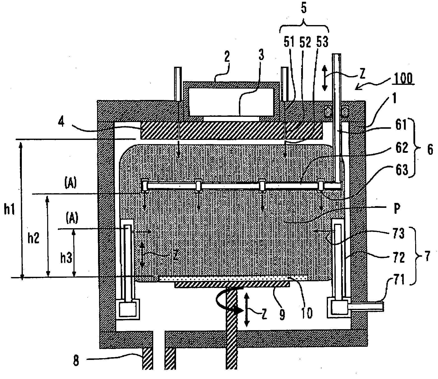
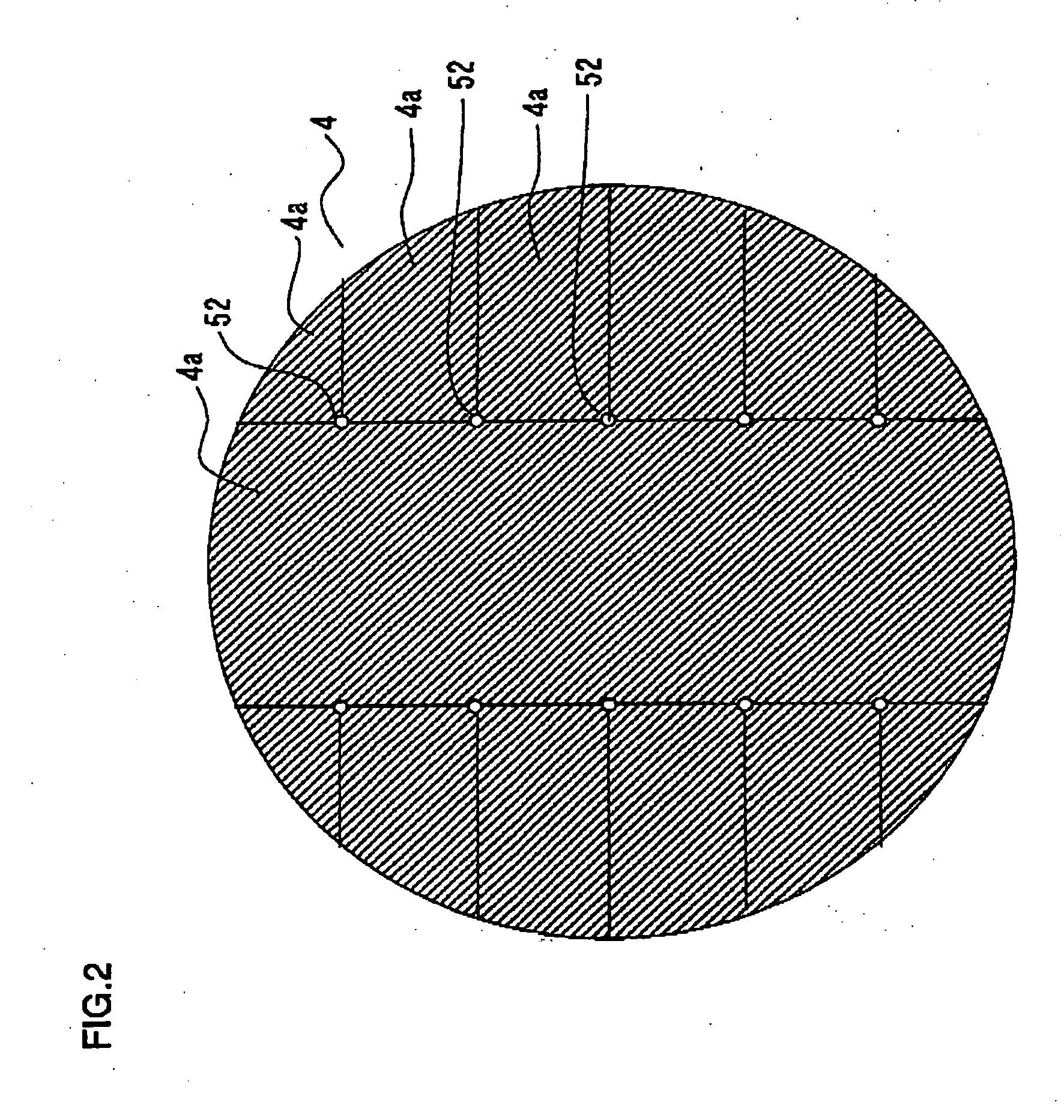
[0025]FIG. 1 is an overall schematic structural view showing the structure of the plasma CVD system according to the first preferred embodiment of the present invention. FIGS. 2 through 4 are, respectively, figures showing the structures of a process gas introduction conduit, an upper surface gas introduction conduit, and a side surface gas introduction conduit in this plasma CVD system according to the first preferred embodiment.

[0026] Referring to FIG. 1, this plasma CVD system 100 comprises a chamber 1, a microwave waveguide 2, a slot antenna 3, a dielectric plate 4, a process gas introduction conduit 5, an upper surface gas introduction conduit 6 for the material gas, a side surface gas introduction conduit 7 for the...


PUM

PropertyMeasurementUnit
Dielectric polarization enthalpyaaaaaaaaaa
Shapeaaaaaaaaaa
Distanceaaaaaaaaaa

Abstract

This surface wave excitation plasma CVD system, along with feeding a material gas including silicon element by feeding the material gas into a chamber 1 from at least one of an upper surface gas introduction conduit and a side surface gas introduction conduit, also activates the material gas with a surface wave excitation plasma and feeds a process gas which initiates chemical reactions within the material gas into the chamber 1 from a process gas introduction conduit 5. A gas feed aperture of the upper surface gas introduction conduit and/or the side surface gas introduction conduit is provided in a position which is closer to the substrate than the gas feed aperture of the process gas introduction conduit.

Description

BACKGROUND OF THE INVENTION [0001] 1. Field of the Invention [0002] The present invention relates to a CVD system which forms a thin film by using a surface wave excitation plasma. [0003] 2. Description of Related Art [0004] In a semiconductor manufacturing process, a plasma CVD system is used which performs thin film manufacture by utilizing a plasma. As such plasma CVD system, in the prior art, a capacitively-coupled plasma (CCP), an inductively-coupled plasma (ICP), an electron cyclotron resonance (ECR—Electron Cyclotron Resonance) plasma processing system, and the like have been used. Furthermore, in recent years, a surface wave excitation plasma (SWP) processing system has come into use, and this can easily generate a plasma of a high density over a wider area than heretofore. [0005] With such a SWP plasma CVD system, first, a material gas which includes an element for the thin film which is to be deposited is fed into the plasma reactive chamber along with a process gas which ...

Claims


Application Information

Patent Timeline
IPC IPC(8): H05H1/46C23C16/00C23C16/40C23C16/42C23C16/455C23C16/511C23C16/517H01L21/205
CPCC23C16/45508C23C16/45563C23C16/511C23C16/45589C23C16/45565H01L21/67207C23C16/4586H01L21/02274
Inventor SUZUKI, MASAYASU
Owner SHIMADZU CORP
Why Eureka
Try Eureka