Semiconductor device including transistors formed in semiconductor layer having single-crystal structure isolated from substrate and fabrication method of the same

Inactive Publication Date: 2005-05-26
KK TOSHIBA
View PDF2 Cites 52 Cited by
  • Summary
  • Abstract
  • Description
  • Claims
  • Application Information

AI Technical Summary

Benefits of technology

[0008] In accordance with one aspect of this invention, a semiconductor device comprises: a substrate; a semiconductor layer of a first conductivity type having a single-crystal structure; a plurality of transistors each including a first gate electrode provided above the semiconductor layer with a first gate insulation film laid therebetween, a pair of impurity regions of a second conductivity type being provided in the semiconductor layer and becoming a drain region and a source region, and a channel body of the first conductivity type provided in the semiconductor layer at a portion between these impurity regions; a first gate line for common connection of the first gate electrodes of the plurality of transistors; a dielectric layer provided above the substrate in an extension direction of the first gate line, for supporting

Problems solved by technology

However, even in the case of using the SOI substrate, when MOS transistors are scaled down and miniatur

Method used


Image

  • Semiconductor device including transistors formed in semiconductor layer having single-crystal structure isolated from substrate and fabrication method of the same
  • Semiconductor device including transistors formed in semiconductor layer having single-crystal structure isolated from substrate and fabrication method of the same
  • Semiconductor device including transistors formed in semiconductor layer having single-crystal structure isolated from substrate and fabrication method of the same

Examples


first embodiment

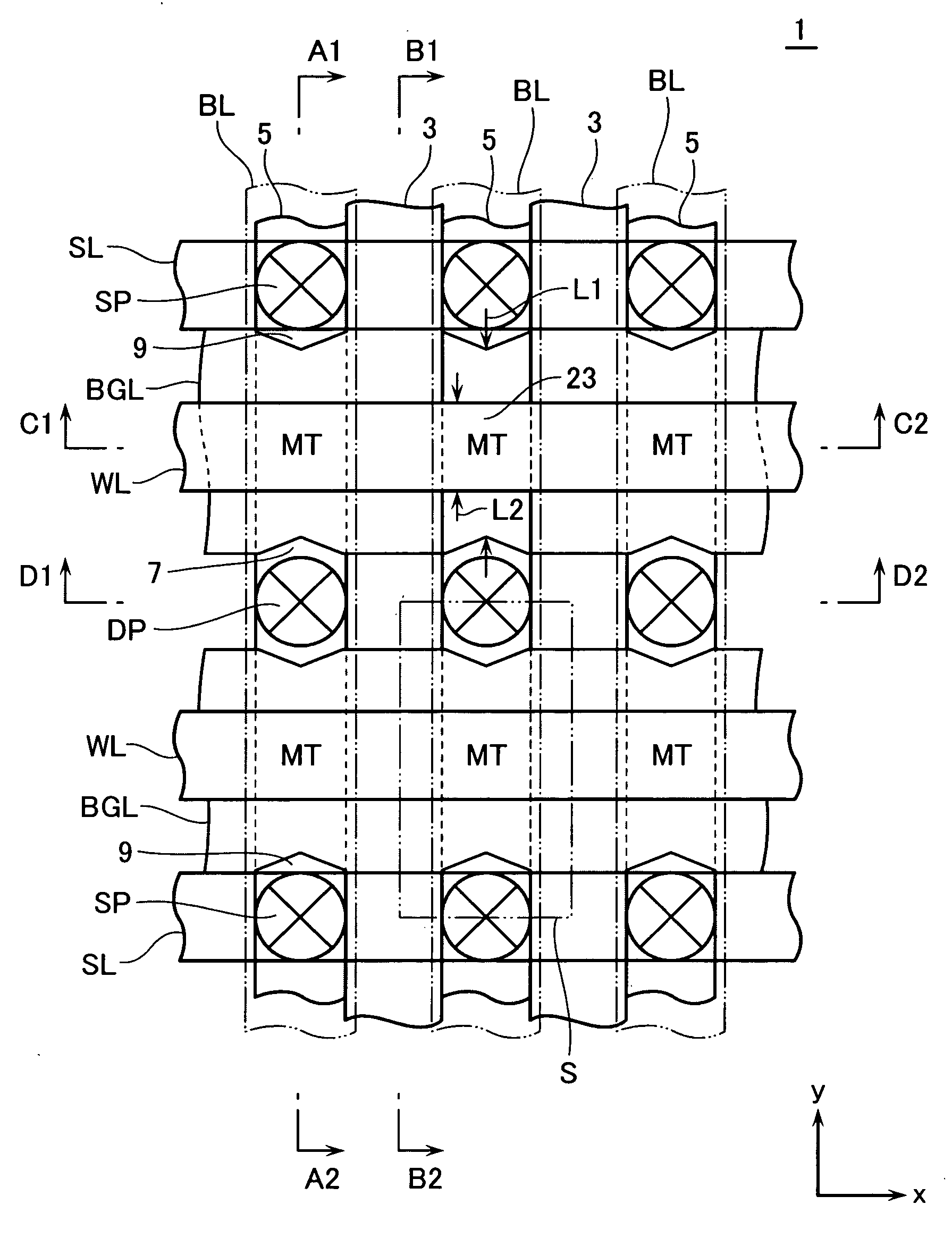
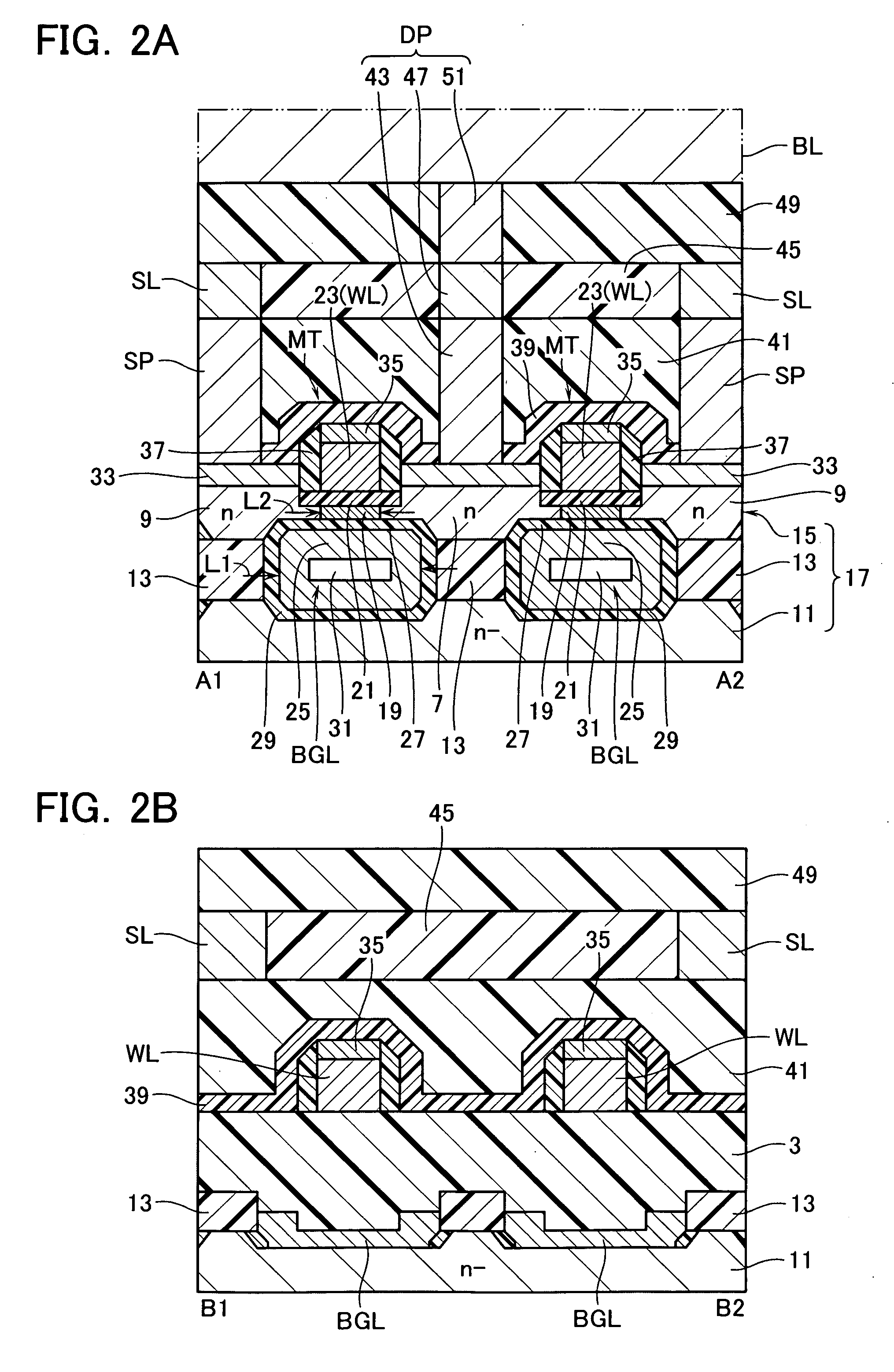
[0095] A semiconductor device in accordance with a first embodiment is an FBC memory. A main feature of this semiconductor device is that it has a structure in which a back gate line extending in a word-line direction is placed between neighboring buried oxide layers that are laid out under a drain region and a source region and extend in the wordline direction. Note that in the first embodiment, a memory transistor functioning as a memory cell means an FBC.

[0096] (Structure of Semiconductor Device)

[0097]FIG. 1 is a diagram showing a plan view of part of a cell array 1 of the semiconductor device in accordance with the first embodiment. The cell array 1 is structured from a plurality of memory transistors MT (or storage transistors MT) which are arranged in a matrix form. A memory transistor MT stores data based on a state of majority carrier accumulated in a channel body that is in an electrically floating state. A layout of the cell array 1 will be explained in detail below.

[00...

second embodiment

[0178] A semiconductor device in accordance with a second embodiment is a transistor 101 making up a logic circuit (referred to hereinafter as a logic transistor). FIG. 33 is a plan view of this transistor 101, which corresponds to FIG. 1. Transistors Q are equivalent to the memory transistors MT of FIG. 1. The logic transistor 101 consists essentially of three transistors Q. Hence, the channel width of a channel body of transistor 101 becomes three times greater than that of a single transistor Q so that it is possible to flow a larger current than the single transistor Q. Thus high-speed operations become attainable.

[0179] Explaining in detail the structure of logic transistor 101, respective front gate electrodes of transistors Q are common-coupled together to a single gate line (one example of the first gate line) GL, while respective back gate electrodes are common-coupled to a single back gate line BGL. In addition, certain ones 103 of the source / drain regions of transistors ...


PUM


Abstract

A semiconductor device includes a substrate, a semiconductor layer of a first conductivity type having a single-crystal structure, and a plurality of transistors each including a first gate electrode provided above the semiconductor layer with a first gate insulation film laid therebetween, a pair of impurity regions of a second conductivity type being provided in the semiconductor layer and each becoming a source or drain region, and a channel body of the first conductivity type provided in the semiconductor layer at a portion between these impurity regions. The device also includes a first gate line for common connection of the first gate electrodes of the transistors, a dielectric layer provided above the substrate in an extension direction of the first gate line, for supporting the semiconductor layer under the pair of impurity regions to thereby dielectrically isolate between the substrate and the semiconductor layer, a second gate electrode provided above the substrate in such a manner as to underlie the channel bodies of the transistors and oppose the channel bodies with a second gate insulation film laid therebetween, the second gate electrode having a gate length larger than a onefold value of a gate length of the first gate electrode and yet less than or equal to thrice the gate length, and a second gate line provided above the substrate along the extension direction of the first gate line while being placed between portions of the dielectric layer underlying the pair of impurity regions, the second gate line being for common connection of the second gate electrode.

Description

CROSS-REFERENCE TO PRIOR APPLICATION [0001] This application is based upon and claims the benefit of priority from the prior Japanese Patent Application No. 2003-394321, filed on Nov. 25, 2003, the entire contents of which are incorporated herein by reference. BACKGROUND OF THE INVENTION [0002] 1. Field of the Invention [0003] The present invention relates to semiconductor devices having transistors formed on a semiconductor substrate such as a silicon-on-insulator (SOI) substrate and also to fabrication methods thereof. [0004] 2. Description of the Related Art [0005] Semiconductor devices are such devices as metal oxide semiconductor (MOS) transistors formed on a semiconductor substrate. Examples of the semiconductor devices are logic circuits and memories such as dynamic random access memory (DRAM). Recently, there is proposed a semiconductor device performing dynamic memory by use of a simpler cell structure for the purpose of replacement of conventional DRAMs (see JP-A-2002-2465...

Claims


Application Information

Patent Timeline
IPC IPC(8): H01L21/8242H01L27/108H01L21/84H01L27/12H01L29/786H01L29/788
CPCH01L21/84H01L27/108H01L29/7881H01L27/1203H01L29/7841H01L27/10802H10B12/20H10B12/00
Inventor SHINO, TOMOAKI
Owner KK TOSHIBA
Why Eureka
Try Eureka