Method for improving a simulation model of photolithographic projection

a simulation model and photolithographic technology, applied in the field of methods for improving the simulation model of the photolithographic projection, can solve the problems of reducing the circuit pattern, the inability to use simulation models in a large-area application, and the errors of two-dimensional models often used

Inactive Publication Date: 2005-05-26
POLARIS INNOVATIONS
View PDF3 Cites 15 Cited by
  • Summary
  • Abstract
  • Description
  • Claims
  • Application Information

AI Technical Summary

Benefits of technology

[0021] In accordance with this procedure, the fit parameter of the filter functio

Problems solved by technology

The projection optical arrangement of the exposure apparatus often contains a plurality of lenses and diaphragms and often reduces the circuit pattern during transfer onto the resist layer.
It has been shown, however, that the two-dimensional models often used are bes

Method used


Image

  • Method for improving a simulation model of photolithographic projection
  • Method for improving a simulation model of photolithographic projection
  • Method for improving a simulation model of photolithographic projection

Examples


Embodiment Construction

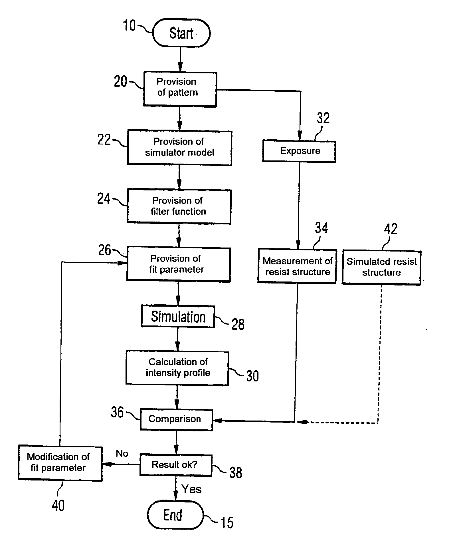
[0025] In accordance with the present invention, an OPC process flow for the calculation of OPC structures of a circuit pattern is described below. An optimization of the geometry of the mask structures and, if appropriate, of further lithography parameters is usually carried out in the OPC process flow. However, the method according to the invention is also suitable for other calculations that require a simulation of a large-area circuit pattern.

[0026]FIG. 1 shows an embodiment of the method according to the invention in the form of a flow diagram. OPC structures serve for altering the linewidth of specific structure elements of the circuit pattern, so that it is possible to compensate for specific imaging errors during the transfer of the circuit pattern into a resist layer of a semiconductor wafer. OPC structures are understood to mean for example structures designated by serifes or hammerheads, likewise including the targeted alteration of linewidths or the addition of fine str...


PUM


Abstract

A method is provided for improving a photolithographic simulation model of the photolithographic simulation of a pattern formed on a photomask. Proceeding from a two-dimensional simulation model that takes account of the physical-chemical processes during lithography, a frequency-dependent intensity loss is calculated which is determined by multiplication of the simulated intensity distribution in the Fourier space by a filter function. An accurate calculation of the intensity distribution in the substrate plane is obtained. This method achieves the accuracy of three-dimensional models with a significantly shorter processing duration and is further suitable in particular for the calculation of OPC structures.

Description

CROSS REFERENCE TO RELATED APPLICATIONS [0001] This application claims priority under 35 USC §119 to German Application No. DE 103 55 264.2, filed on Nov. 26, 2003, and titled “Method for Improving a Simulation Model of Photolithographic Projection,” the entire contents of which are hereby incorporated by reference. FIELD OF THE INVENTION [0002] The invention relates to a method for improving a simulation model of the photolithographic projection of a pattern formed on a photomask onto a substrate of a semiconductor wafer. BACKGROUND [0003] For the fabrication of integrated circuits, layers provided with different electrical properties are usually applied on semiconductor wafers and in each case patterned lithographically. A lithographic patterning step may consist in applying a photosensitive resist, exposing the latter with a desired structure for the relevant plane and developing it, and then transferring the resultant resist mask into the underlying layer in an etching step. [00...

Claims


Application Information

Patent Timeline
IPC IPC(8): G03F1/00G03F1/36G03F7/20G05B17/00G06F17/50
CPCG03F1/144G03F7/705G03F7/70441G03F1/36
Inventor KUCHLER, BERNDZIEBOLD, RALFNOLSCHER, CHRISTOPH
Owner POLARIS INNOVATIONS
Why Eureka
Try Eureka