

Processed body carrying device, and processing system with carrying device
a processing system and carrying device technology, applied in the field of transfer mechanisms, can solve the problems of large-scale increase in strength, deterioration in throughput, and enlargement of the size of the common vessel, and achieve the effect of convenient increase or decrease of the number of processing apparatuses connected to the main transferring mechanism (via the respective individual transferring chambers)
- Summary
- Abstract
- Description
- Claims
- Application Information
AI Technical Summary
Benefits of technology
Problems solved by technology
Method used
Image

Examples
Embodiment Construction
[0039] Hereinafter, a preferred embodiment of a transfer mechanism of an object to be processed and a processing system in accordance with the present invention will be described in detail with reference to the accompanying drawings.
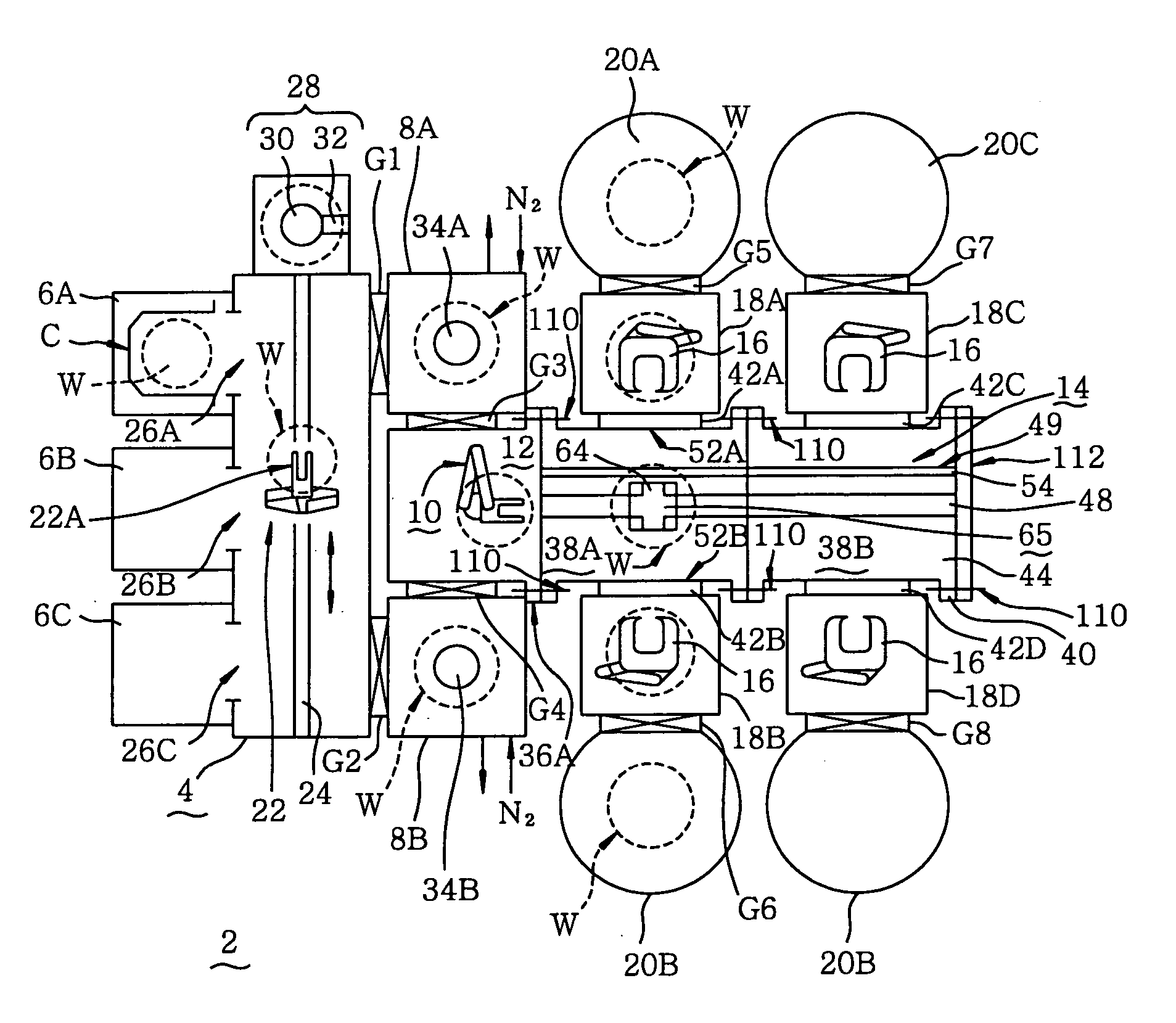
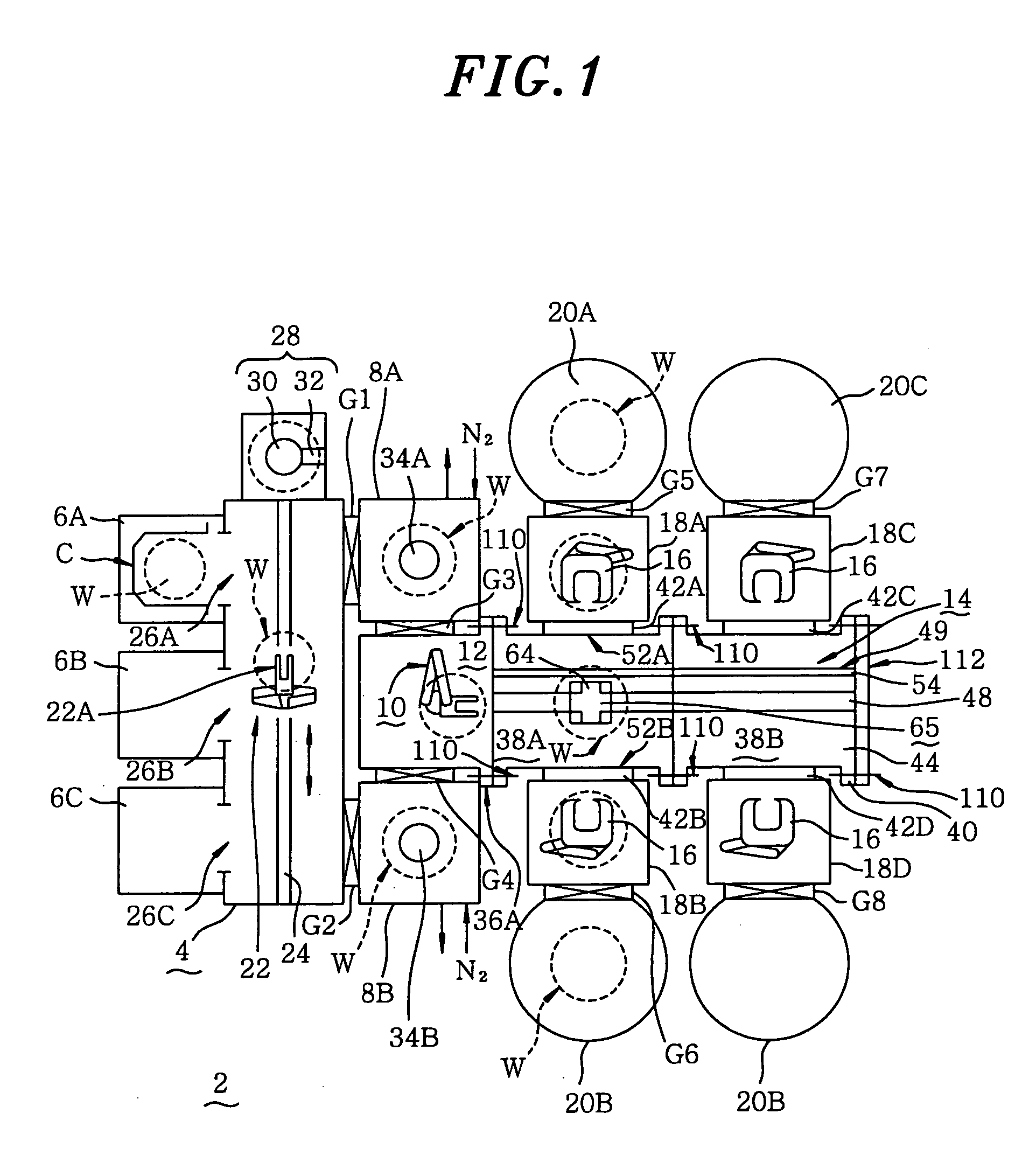
[0040] Referring to FIG. 1, a processing system 2 is provided with a main transfer mechanism 14, an auxiliary transfer mechanism 12, two load-lock mechanisms 8A and 8B, an entrance transfer mechanism 4, three cassette stations 6A, 6B and 6C, four individual transfer mechanisms 18A to 18D and four processing apparatuses 20A to 20D.
[0041] The main transfer mechanism 14 includes a casing 40 for defining a main transfer chamber 44 under a vacuum state, the casing 40 having two sets of transfer ports 52A, 52B and 52A, 52B. The auxiliary transfer mechanism 12 includes a casing for defining an auxiliary transfer chamber under a vacuum state which can communicate with the main transfer chamber 44; and an auxiliary transfer unit 10 installed in the transfer cha...
PUM
| Property | Measurement | Unit |
|---|---|---|
| included angle | aaaaa | aaaaa |
| vacuum state | aaaaa | aaaaa |
| height | aaaaa | aaaaa |
Abstract
Description
Claims
Application Information