Flat panel display

a display panel and flat panel technology, applied in the direction of discharge tube luminescnet display, discharge tube/lamp details, electric discharge lamps, etc., can solve the problems of pin hole or open circuit defects still generating, image quality deterioration, and high heat generation, so as to prevent defects from occurring

Active Publication Date: 2005-06-02
SAMSUNG DISPLAY CO LTD
View PDF18 Cites 42 Cited by
  • Summary
  • Abstract
  • Description
  • Claims
  • Application Information

AI Technical Summary

Benefits of technology

[0018] In an exemplary embodiment according to the present invention, a flat panel display capable of preventing defects from occurring by decreasing a taper angle at an edge of an anode, is provided.

Problems solved by technology

In addition, the organic emission layer has not been deposited on the stepped portions of the anode and near the contact hole and via hole, or it has not been uniformly deposited to thereby have a thickness thinner than those of other portions.
Due to the occurrence of the dark spots, emission regions become reduced to thereby deteriorate image quality.
Thus, when a high voltage is applied between the anode and the cathode, the portion that is not densely deposited has a void in the cathode due to electromigration resulting from the current density concentration, so that high heat occurs due to a resistance increase resulting from external oxygen penetration.
However, pin hole or open circuit defects still generate near the contact hole, the via hole, or in the stepped portion as shown in FIG. 4 and FIG. 5, and dark spots are also generated due to the cathode that is not densely deposited.
By way of example, the organic emission layer and the cathode are likely to be deteriorated at the edge of the opening when the taper angle is large, and there is a limit to reducing the taper angle and the thickness of the pixel defining layer because of a parasitic capacitance and a step resulting from wiring when the taper angle is small.
Further, an aperture ratio is further decreased with the increasing use of the pixel defining layer, and outgas from the pixel defining layer causes the emission region to be reduced, which leads to pixel size reduction, so that lifetime and image quality are deteriorated, and additional processes for depositing and etching the pixel defining layer are required.

Method used


Image

  • Flat panel display
  • Flat panel display
  • Flat panel display

Examples


Embodiment Construction

[0050] The present invention will now be described more fully hereinafter with reference to the accompanying drawings, in which certain exemplary embodiments of the present invention are shown. This invention may, however, be embodied in different forms and should not be construed as being limited to the embodiments set forth herein. In the drawings, the thickness of layers and regions are exaggerated for clarity. Like reference numerals / characters designate like elements throughout the specification and the drawings.

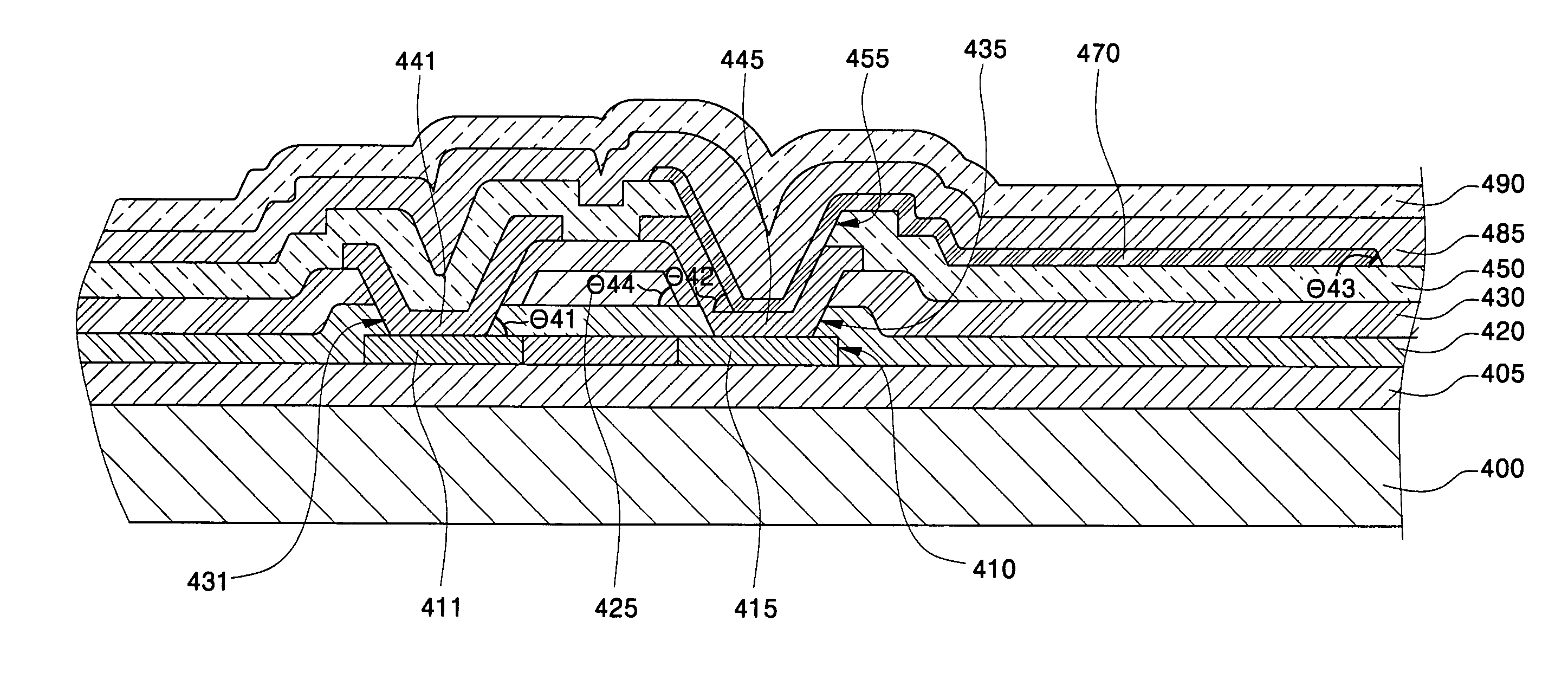
[0051] Referring to FIG. 7, a buffer layer 405 is formed on an insulating substrate 400, and a semiconductor layer 410 having source and drain regions 411 and 415 is formed on the buffer layer 405. A gate electrode 425 is formed on the gate insulating layer 420, and source and drain electrodes 441 and 445 are formed on an interlayer insulating layer 430, and are connected to the source and drain regions 411 and 415 through contact holes 431 and 435, respectively.

[0052...


PUM


Abstract

A flat panel display capable of reducing element defects by decreasing taper angles of contact holes and a via hole. The flat panel display includes a thin film transistor having at least source and drain electrodes formed over an insulating substrate, an insulating layer having a via hole for exposing one of the source and drain electrodes, and an anode connected to said one of the source and drain electrodes through the via hole. The via hole and the anode are tapered with taper angles of 60° or less. The source and drain electrodes are connected respectively to source and drain regions of the thin film transistor through the contact holes. The contact holes are also tapered with taper angles of 60° or less.

Description

CROSS-REFERENCE TO RELATED APPLICATION [0001] This application claims priority to and the benefit of Korean Patent Application No. 2003-84786, filed Nov. 27, 2003, the disclosure of which is incorporated herein by reference in its entirety. BACKGROUND OF THE INVENTION [0002] 1. Field of the Invention [0003] The present invention relates to a flat panel display and, more particularly, to a full color active matrix organic light emitting display (AMOLED), which lowers taper angles of an anode and a via hole to prevent defects from occurring. [0004] 2. Description of the Related Art In general, AMOLED has a plurality of pixels arranged on a substrate in a matrix format, and each pixel includes an electroluminescent (EL) element with an anode, an organic emission layer, and a cathode that are layered together. The AMOLED also includes a thin film transistor (TFT) connected to the EL element as an active element for driving the EL element. [0005]FIG. 1 is a cross-sectional view of a bott...

Claims


Application Information

Patent Timeline
Patent Type & Authority Applications(United States)
IPC IPC(8): H01L21/28H05B33/02H01L21/768H01L21/77H01L21/84H01L27/12H01L27/32H01L29/417H01L29/786H01L51/50H01L51/52H05B33/22
CPCH01L21/76804H01L27/12H01L27/3248H01L27/1248H01L29/41733H01L51/5206H01L27/1244H01L27/3262H10K59/123H10K59/1213H10K50/813H05B33/22
Inventor KIM, MU-HYUNSONG, MYUNG-WONCHO, YU-SUNG
Owner SAMSUNG DISPLAY CO LTD
Why Eureka
Try Eureka