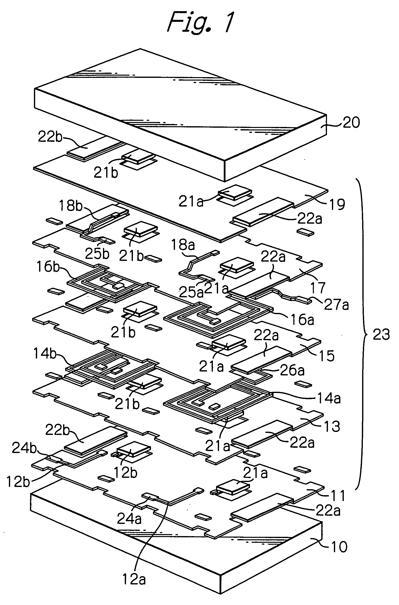
[0009] It is therefore an object of the present invention to provide a thin-film common mode filter and a thin-film common mode filter array possessing an improved reliability in the
electrical connection between the drawing terminals and the external-connect
electrode terminals.
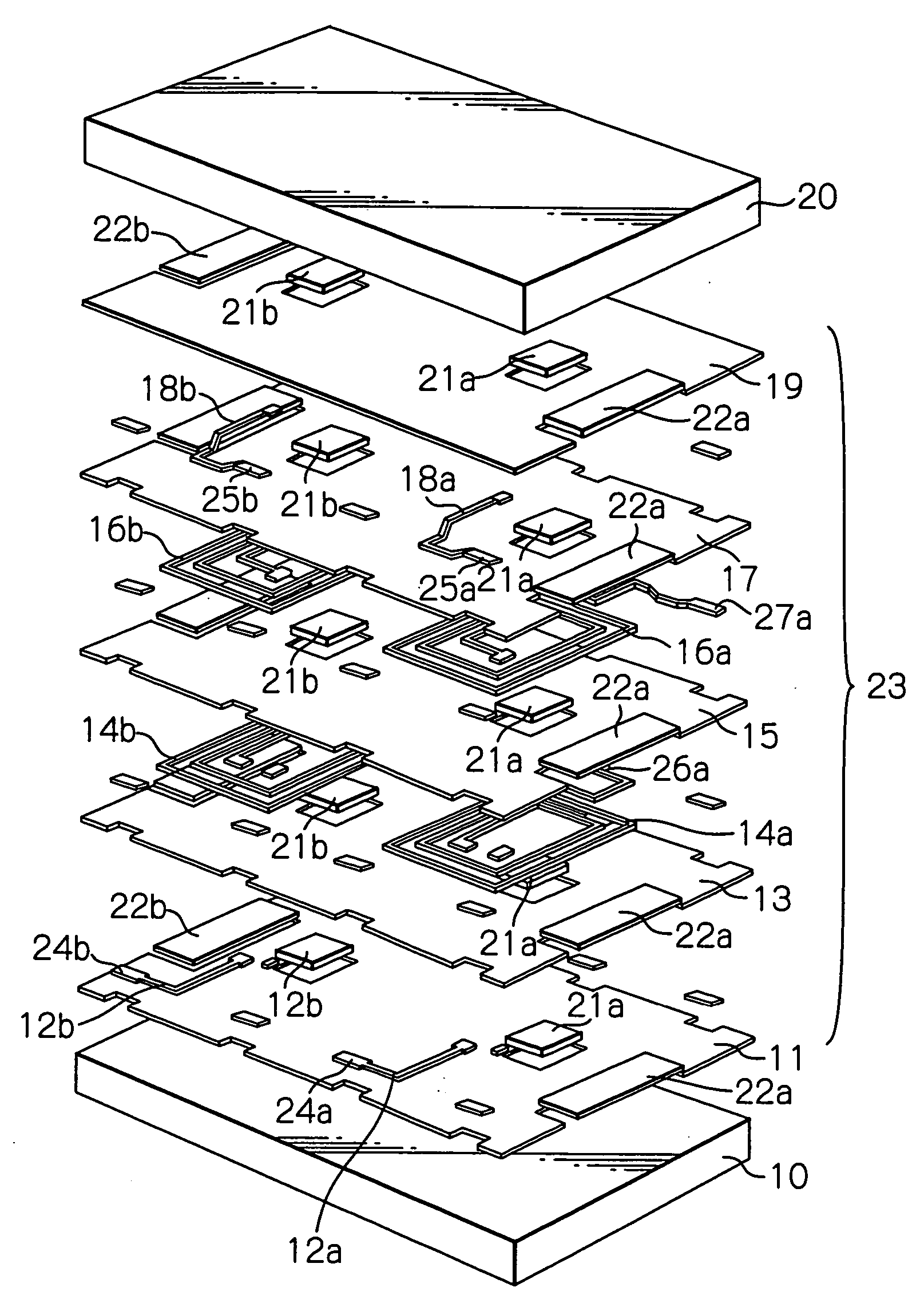
[0011] Each of the drawing terminal is formed by stacking a plurality of the conductor
layers to be patterned into the lower
lead conductor, the lower coil conductor, the upper coil conductor and the upper
lead conductor and bringing the conductor
layers into conduction with each other. Therefore, because the side cross-sectional area of the drawing terminal, or the exposed area on the
chip side, becomes larger, the drawing terminals and the external-connect
electrode terminals have a much excellent electric connection between them, and a reliability in electric connection is greatly improved.
[0014] More preferably, in the case, centers of the through holes in the first layer to the third layer coincide with each other. Then, the through holes in the first layer to the third layer may have the same form and the same dimension as each other, further more preferably, the through holes in the first layer to the third layer, that is, in the lower layer to the upper layer have sequentially larger dimensions. When the through holes have the same dimension as each other, the drawing terminal portion has a large step, then some insulating material is likely to remain in the through holes under an influence of reflections during
exposure in
photolithography, and therefore, a reliability in conduction is reduced (Especially, this problem becomes marked in the case of a high aspect-ratio pattern). However, by making the through holes in the lower layer to the upper layer sequentially larger, the step becomes smaller, and therefore, a reliability in the conduction between the layers is improved.
[0015] It is also preferable that each center position of the through holes in the first layer to the third layer is alternately changed. In the case, more preferably, the through holes in the first layer to the third layer have the same form and the same dimension as each other. By alternately changing the position of each center of the through holes, the
dimple of the conductor in the through hole becomes smaller, then the surface of the insulating layer thereon becomes flatter, and therefore, the surfaces of the through hole conductors and of the insulating layers formed subsequently also become flatter. Consequently, a reliability in the conduction between the layers is improved, and the step becomes smaller.
[0016] Preferably, widths (W1) of said upper and lower lead conductors are less than twice the widths (W2) of said upper and lower coil conductors (W1<2W2). The higher aspect ratios (height / width) of the coil pattern and of the lead pattern cause smaller capacities between the coil conductors and between the coil conductor and the
lead conductor. As the results, the high-frequency
transmission properties are improved. However, the higher
aspect ratio design makes it difficult to narrow the spacing between the lead conductor and the coil conductor. To solve the difficulty, narrowing the width of the lead conductor is effective. However, setting the width of the lead conductor (W1) not less than twice the width of the coil conductor (W2) lowers the
resonance frequency to a large degree. Therefore, by setting W1<2W2, the thin-film common mode filter showing less decrease in the
resonance frequency can be provided.
[0017] Preferably, the lower and upper lead conductors are formed of a
copper (Cu) whose external surfaces are covered with
nickel(Ni) /
chromium(Cr) films. In the case, more preferably, a surface of the lower lead conductor in a connection portion between the lower coil conductor and the lower lead conductor, and a surface of the upper lead conductor in a connection portion between the upper coil conductor and the upper lead conductor, are covered with only
chromium (Cr) films. A trouble of an electric resistance increase caused by the
diffusion between Cu / Ni can be avoided because Ni is eliminated in the connection portion.

