Spatial light modulator, spatial light modulator array, and exposure apparatus

Inactive Publication Date: 2005-06-02
FUJIFILM HLDG CORP +1
View PDF1 Cites 20 Cited by
  • Summary
  • Abstract
  • Description
  • Claims
  • Application Information

AI Technical Summary

Benefits of technology

[0016] In this spatial light modulator, the movable member is formed from a displaceable beam having an optical function film and a conductive section. The fixed drive electrode is disposed outside a range of rotational path within which mechanical displacement of the movable member becomes feasible; that is, outside a range of displacement path in which structural displacement can be made possible not by controlling a drive voltage but by external force. As a result, electrostatic attracting force is exerted between the movable member and the fixed drive electrode, by means of applying a drive voltage to the conductive section of the movable member and the fixed drive electrode, and the movable member is actuated and displaced toward the fixed drive electrode in a non-contacting manner and can be brought to a standstill. Thereby, the light radiated on the optical function film can be modulated. As mentioned above, non-contact displacement of the optical function film becomes feasible. Moment of inertia is made smaller by reducing the overall mass of the movable section, thereby enabling high-speed driving at a low voltage.
[0056] In this exposure apparatus, the optical function film can be displaced without occurrence of contact between the movable member and the fixed drive electrode, both belonging to the spatial light modulator. Fixing of the movable element to the fixed drive electrode is prevented, and improved reliability of the element and improved durability of the exposure apparatus are achieved. Moreover, since the footprint of the drive structure is small, there can be obtained an exposure apparatus having a high utilization factor of light.

Problems solved by technology

However, since the landing piece of the yoke comes into contact with the lower address electrode, there arises van der Waals force or adhesion of the landing piece to the address electrode by means of impurities or an organic-based gas in the environment, thereby resulting in a problem of a decrease in the reliability of an element.
As a result, the overall mass of the movable section is increased, thereby posing a limitation on high-speed movement.
As a result, the electrostatic attractive force acting on the pixel mirror and the address electrodes and the electrostatic attractive force acting on the yoke and the address electrodes become smaller, thus posing a limitation on the tendency toward lower voltage and higher-speed driving.
Further, since a single trap electrode operates only the edge, there arises an inconvenience of a reduction in a range of action of an electric field to be trapped.
Hence, the footprint of the comb drive structure becomes larger, thereby posing difficulty in attaining miniaturization and an increase in resolution and a problem of a low utilization factor of light.

Method used


Image

  • Spatial light modulator, spatial light modulator array, and exposure apparatus
  • Spatial light modulator, spatial light modulator array, and exposure apparatus
  • Spatial light modulator, spatial light modulator array, and exposure apparatus

Examples


first embodiment

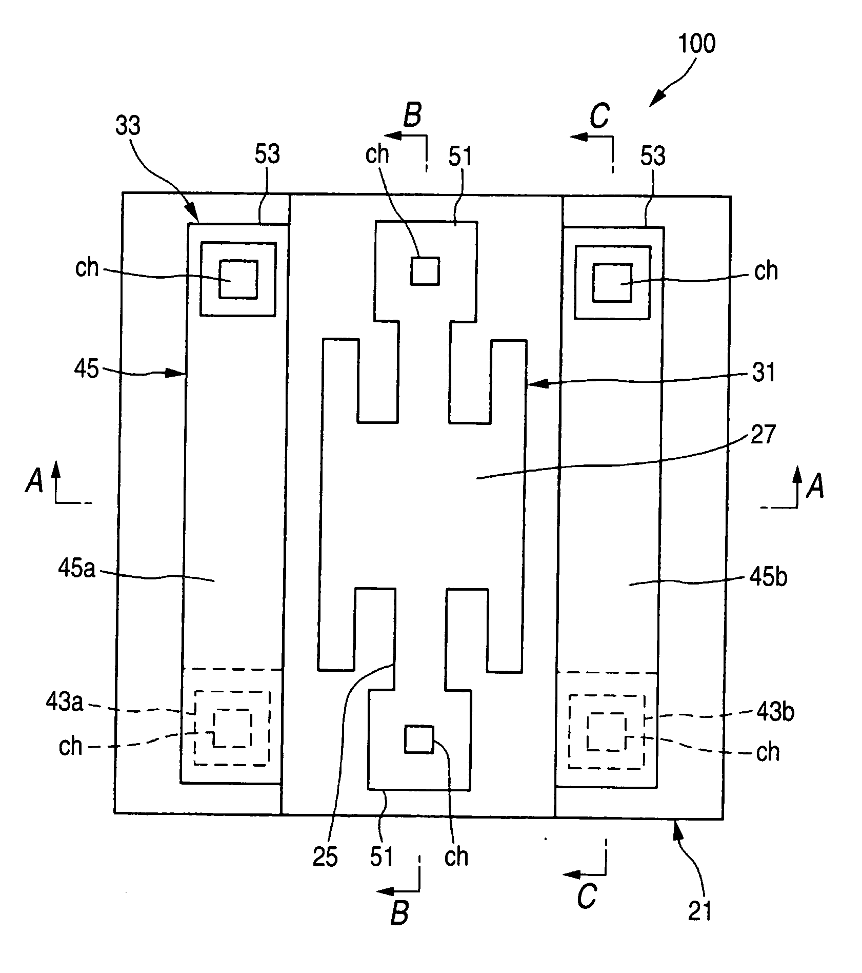
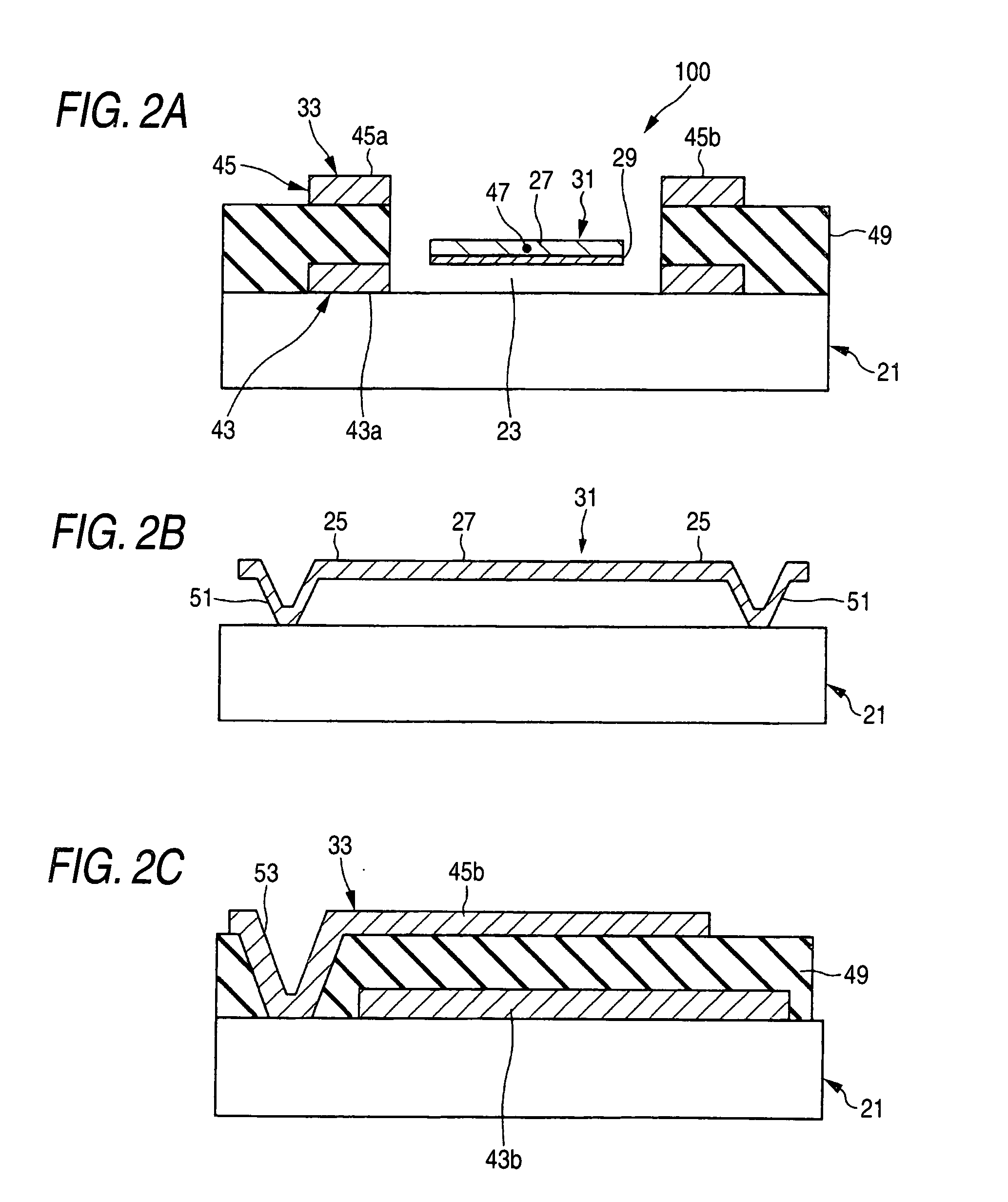
[0100]FIG. 1 is a plan view of a spatial light modulator according to the present invention; FIGS. 2A to 2C are cross-sectional views, wherein FIG. 2A is a cross-sectional view taken along line A-A shown in FIG. 1, FIG. 2B is a cross-sectional view taken along line B-B shown in FIG. 1, and FIG. 2C is a cross-sectional view taken along line C-C shown in FIG. 1; FIG. 3 is across-sectional view of the substrate shown in FIG. 1; and FIG. 4 is an electrode wiring diagram of the spatial light modulator shown in FIG. 1.

[0101] As shown in FIGS. 1 and 2, a spatial light modulator 100 of the present embodiment has, as a basic structural elements, a substrate 21, a movable member 31 having a light reflector (hereinafter also called a “mirror section”) 27 and a conductive section 29 provided in at least a portion of the movable member, and a fixed electrode 33. In the light reflector 27, a beam 25 (also called a “hinge”) is provided so as to hang across the substrate 21 by way of a void 23, and...

second embodiment

[0151] A spatial light modulator according to the present invention will now be described.

[0152]FIG. 8 is a plan view of the spatial light modulator of the second embodiment attached to the beam of a separate mirror section, and FIG. 9 is a cross-sectional view taken along line D-D shown in FIG. 8. In embodiments and modifications provided below, those elements which are the same as those shown in FIGS. 1 through 7 are assigned the same reference numerals, and repeated explanations thereof are omitted.

[0153] In a spatial light modulator 200 of the present embodiment, a movable member 63 differs from the movable member 31. Specifically, the light reflector is embodied as a separate mirror section 65 attached to the hinge 25. The mirror section 65 is provided at least at an entrance opening section formed in the hinge 25. For instance, the mirror section 65 is newly formed, on the hinge 25 made of metal such-as aluminum, from the same material as that of the hinge 25. The mirror sect...

third embodiment

[0168] A spatial light modulator according to the present invention will now be described.

[0169]FIG. 13 is a plan view of a third embodiment of a spatial light modulator according to the present invention; FIGS. 14A to 14C are cross-sectional views, wherein FIG. 14A is a cross-sectional view taken along line E-E shown in FIG. 13, FIG. 14B is a cross-sectional view taken along line F-F shown in FIG. 13, and FIG. 14C is a cross-sectional view taken along line G-G shown in FIG. 13; and FIG. 15 is a electrode wiring diagram of the spatial light modulator shown in FIG. 13.

[0170] A spatial light modulator 300 of the present embodiment has the substrate 21; a movable member 73 having the hinge 25 provided so as to hang across the substrate 21, the mirror section 27 which is a light reflector capable of being vertically displaced by means of flexure of the hinge 25, and the conductive section 29 provided in at least a portion of the movable member; and the fixed electrode 33 disposed outsi...


PUM


Abstract

A spatial light modulator has a substrate; a movable member which is disposed so as to hang across the substrate in a displaceable manner and has a conductive section provided in at least a portion of the movable member; an optical function film which follows mechanical displacement of the movable member and is fixed to the same; and a drive fixed electrode which is disposed outside a range of mechanical displacement of the movable member and displaces and drives the movable member. Electrostatic attractive force is generated between the movable member and the driving fixed electrode by applying a drive voltage between the conductive section of the movable member and the driving fixed electrode, thereby displacing and driving the movable member, bringing the same into a stationary state in a non-contacting manner, and modulating light radiated on the optical function film.

Description

BACKGROUND OF THE INVENTION [0001] 1. Field of the Invention [0002] The present invention relates to a spatial light modulator, a spatial light modulator array, and an exposure apparatus using them. [0003] 2. Description of the Related Art [0004] A spatial light modulator (SLM) is a device for forming an optical image corresponding to an electrical or optical input. One type of SLM is a digital micromirror device (DMD) in which a micromirror is fabricated by means of a micro-mechanics technique and which attempts to deflect light by tilting the micromirror. The DMD is a monolithic single chip integrated circuit SLM and is constituted of a high-density array of movable micromirrors, each of which measures, e.g., 16 microns square. These mirrors are formed on an address circuit, thereby forming a pixel of the DMD array. When set at one of two positions the mirrors reflect incident light toward a projection lens, and when set at the other position deflect the incident light toward a li...

Claims


Application Information

Patent Timeline
IPC IPC(8): B81B3/00B81B7/04G02B26/08
CPCG02B26/0841
Inventor KIMURA, KOICHISUMI, KATSUTO
Owner FUJIFILM HLDG CORP
Why Eureka
Try Eureka