Write driver circuit in phase change memory device and method for applying write current

a write driver and memory device technology, applied in semiconductor devices, digital storage, instruments, etc., can solve the problems of degrading affecting the reliability of the write operation, so as to achieve the effect of convenient write operation

Active Publication Date: 2005-06-02
SAMSUNG ELECTRONICS CO LTD
View PDF5 Cites 72 Cited by
  • Summary
  • Abstract
  • Description
  • Claims
  • Application Information

AI Technical Summary

Benefits of technology

[0036] In the write driver circuit in the phase change memory device and the method for applying a write current of the present invention, the write operation is performed more easily even in the case where there occurs a current output shift in the write current generation circuit or where the phase change memory cell having the phase change material has a phase change property shift due to an external factor or a process change.

Problems solved by technology

However, there is a potential problem that a “current output shift” can occurs in a write current generation circuit, such as a write driver circuit or the like.
Thus, if the current output from the write current generation circuit, such as a write driver circuit or the like, is not generated as a predefined value, e.g., due to the external factor or process change, current levels of the reset pulse and the set pulse will not be generated as predefined values, thereby degrading the reliability of the write operation.
Further, in the case where the phase change memory cell having the phase change material has a “phase change property shift”, e.g., due to an external factor or process change, it is difficult to guarantee the reliability of the write operation even though the current levels of the reset and set pulses are applied with the predefined value.
If the reliability of the write operation is degraded, it will reduce manufacture yield in production of the phase change memory device.

Method used


Image

  • Write driver circuit in phase change memory device and method for applying write current
  • Write driver circuit in phase change memory device and method for applying write current
  • Write driver circuit in phase change memory device and method for applying write current

Examples


first embodiment

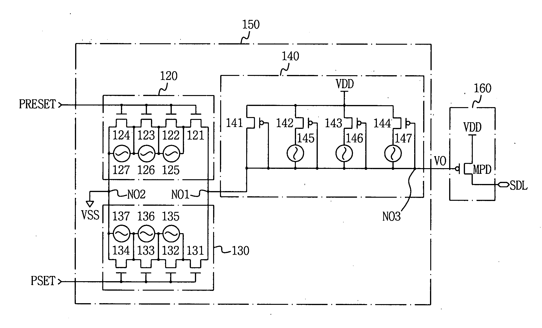
[0058]FIG. 8 is a circuit diagram showing circuit details of the write current control unit 150 and the current driving unit 160 of FIG. 6. The node NO1 corresponds to a current supply terminal and the node NO2 is a ground. Current will flow from current supply terminal node NO1 through a selected one of the reset current control unit 120 and the set current control unit 130, to the ground NO2 .

[0059] Referring to FIG. 8, a reset current control unit 120 is composed of first to fourth N-type (e.g., NMOS) transistors 121 to 124, and first to third fuses 125 to 127. The first to fourth N-type (e.g., NMOS) transistors 121 to 124, which are serially connected (at their drain-source channels), receive the first selection pulse signal PRESET via their respective gate terminals. The first to third fuses 125 to 127 are correspondingly connected to the (drain of source) terminals of the second, third and fourth NMOS transistors. For example, when the first fuse 125 is cut (blown), a current ...

second embodiment

[0072]FIG. 10 is a circuit diagram showing the write current control unit and current driving unit 150 of FIG. 6. Referring to FIG. 10, a reset current control unit 120-1 is composed of first to fourth N-type (e.g., NMOS) transistors 121 to 124, and fifth and sixth N-type (e.g., NMOS) transistors 128 and 129. The first to fourth NMOS transistors 121 to 124, of which are serially connected to one another (drain-to-source, receive the first selection pulse signal PRESET in common at their respective gate terminals. The fifth NMOS transistor 128 is connected in parallel with the first and second NMOS transistors 121 and 122, and the sixth NMOS transistor 129 is connected in parallel with the third and fourth NMOS transistors 123 and 124. For example, if the fifth NMOS transistor 128 is turned on, the current flowing at the drain of the first NMOS transistor 121 also flows through the drain-source channel of the fifth NMOS transistor 128. Control signals A and B are applied to the gate ...

third embodiment

[0082]FIG. 12 is a circuit diagram showing the write current control unit and current driving unit 150 of FIG. 6. Referring to FIG. 12, a reset current control unit 120-2 is composed of first to fourth N-type (e.g., NMOS) transistors 121 to 124, and fifth and sixth NMOS transistors 127 and 128. The first to fourth NMOS transistors 121 to 124, are serially connected with one another (drain-to-source), between node NO1 and ground (NO2). The first to fourth NMOS transistors 121 to 124, and fifth NMOS transistor 127, receive the first selection pulse signal PRESET in common at their respective gate terminals. The source terminal of the sixth NMOS transistor 128 is connected to the ground (node NO2 ), and its drain terminal is connected to node NO1 through the source-gate channel of the fifth NMOS transistor 127, and its gate terminal is connected to control signal DC-RESET. For example, according to a voltage level of the control signal DC-RESET applied to the gate terminal of the sixth...


PUM


Abstract

A write driver circuit including a plurality of programmable fuses for a phase change memory device in which a write operation is correctly performed even in the case where a current output shift in a write current generation circuit; or in the case where a phase change memory cell has a phase change property shift due to an external factor or due a process change. The write driver circuit includes; a write current control unit for outputting a first or second level of voltage selected, by selecting one of a first or second programmable current path, based on whether a first or second selection pulse signal is applied; and a current driving unit for generating a write current controlled by the output voltage of the write current control unit. Each of the first and second programmable current paths includes fuses that can be programmed to adjusted their resistance to adjust the respective selected output voltage to compensate for a current output shift in a write current generation circuit or for a phase change memory cell has a phase change property shift.

Description

CROSS-REFERENCE TO RELATED APPLICATION [0001] This application claims the benefit of Korean Patent Application No. 2003-0084873, filed on Nov. 27, 2003, the disclosure of which is hereby incorporated herein by reference in its entirety. BACKGROUND [0002] 1. Technical Field [0003] The present invention relates to a phase-change memory device. More particularly, the present invention relates to a write driver circuit in a phase change memory device and a method for applying a write current. [0004] 2. Discussion of the Related Art [0005] Random Access Memory (RAM) is commonly used to store data in electronic systems, such as a computer system, communication equipment, digital cameras, and other electronic devices. [0006] A non-volatile RAM memory cell may include a phase change material. Phase change memory devices use phase change materials, i.e., materials that can be electrically switched between a generally amorphous and a generally crystalline state, for electronic memory applicat...

Claims


Application Information

Patent Timeline
Patent Type & Authority Applications(United States)
IPC IPC(8): G11C13/00G11C13/02G11C16/02G11C16/12G11C16/30G11C29/02H01L27/105H01L45/00
CPCG11C13/0004G11C13/0038G11C13/0069G11C2213/79G11C29/028G11C2013/0078G11C2029/5006G11C29/02G11C13/02
Inventor CHO, BEAK-HYUNGKWAK, CHOONG-KEUN
Owner SAMSUNG ELECTRONICS CO LTD
Why Eureka
Try Eureka