Clock generator

Inactive Publication Date: 2005-06-09
MONTEREY RES LLC
View PDF8 Cites 12 Cited by
  • Summary
  • Abstract
  • Description
  • Claims
  • Application Information

AI Technical Summary

Benefits of technology

[0016] The present invention has been made to resolve at least one of the above-mentioned problems. The present invention intends to provide a clock generator of which modu

Problems solved by technology

Any technology disclosed in JP Laid-open Patent Publication No. 2000-101424 accompany increase power consumption at a clock generator circuit, which is problematic.
An operational amplifier and a comparator require bias current flowing constantly in terms of

Method used


Image

  • Clock generator
  • Clock generator
  • Clock generator

Examples


Example

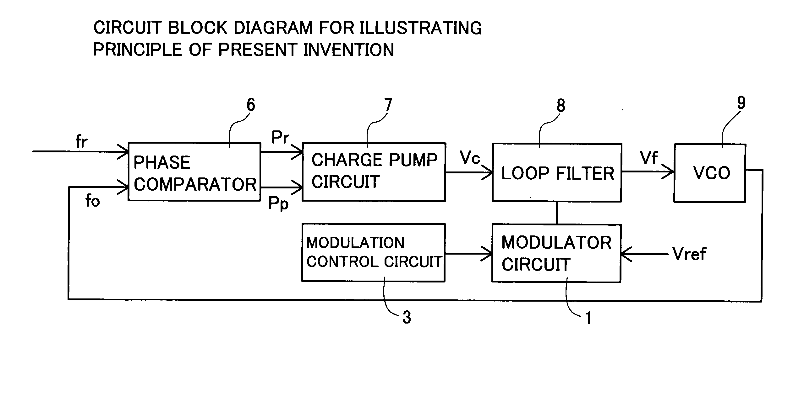
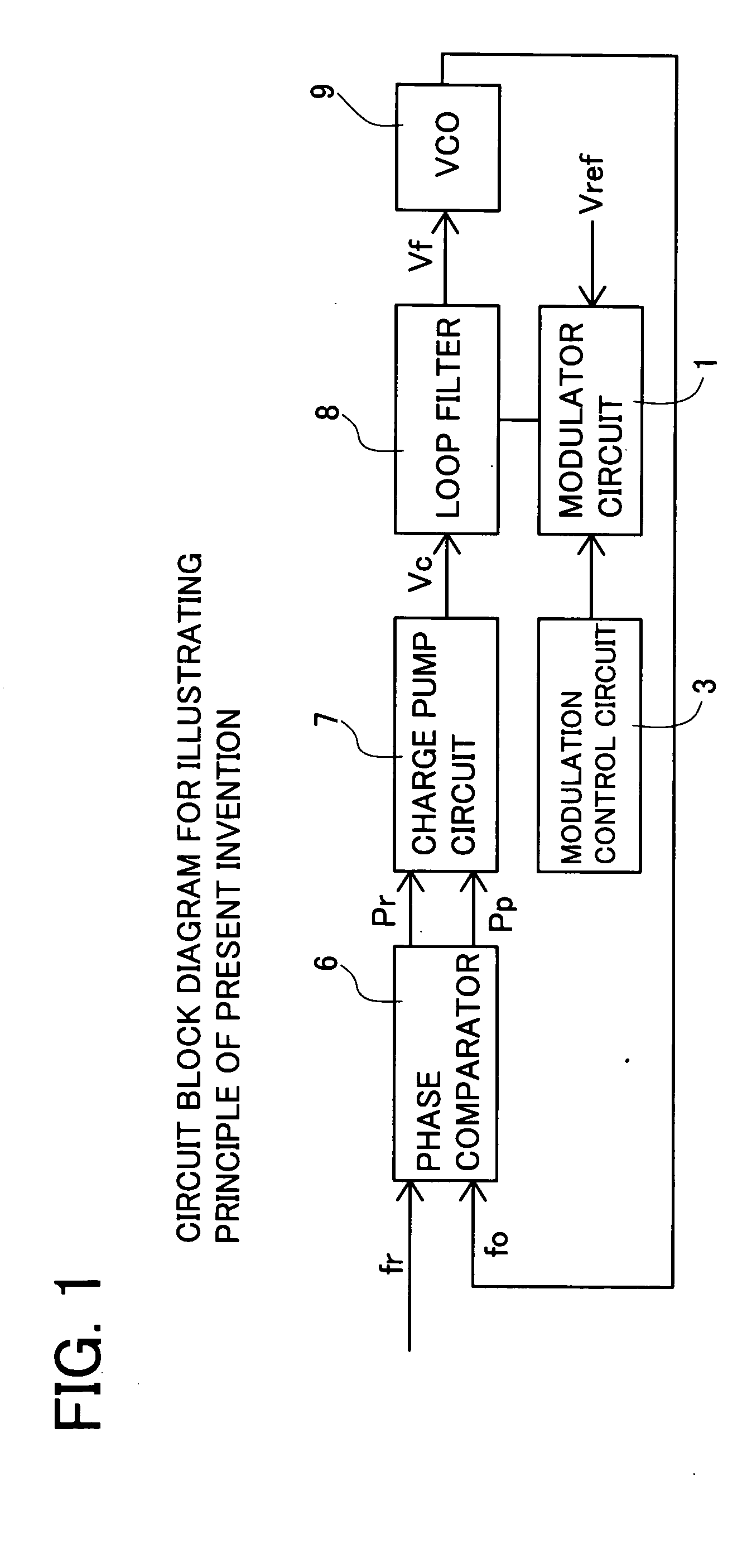
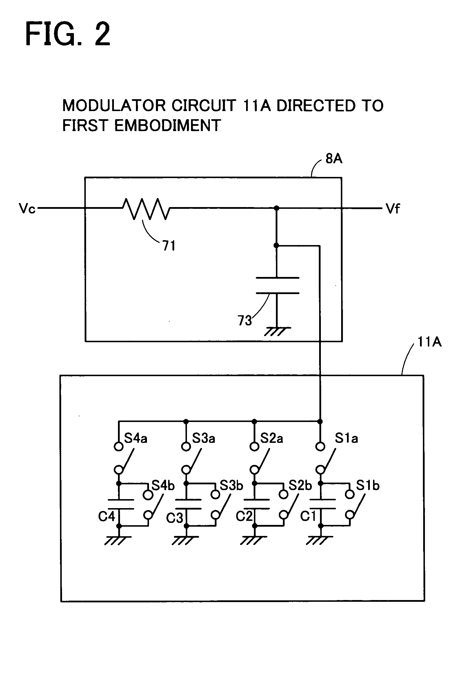
[0041]FIGS. 2, 3 show modulator circuits 11A, 11B of the first embodiment and at the same time, the circuit structure of a loop filter (LPF) 8A and the relation of connection between the both circuits. The loop filter (LPF) 8A is an example of the structure of a low pass filter in which an output signal Vc outputted from the charge pump circuit 7 is inputted to a resistor device 71 and smoothed by a capacitance device 73. The inputted output signal Vc is smoothed and outputted as the phase balanced voltage Vf.

[0042] In the modulator circuits 11A, 11B, plural capacitance devices C1-C4 each in which a terminal thereof is connected to 0V are provided in parallel. The other terminal of each of the capacitance devices C1-C4 is connected to a terminal of a capacitance device 73 within the loop filter (LPF) 8A through respective switch devices S1a-S4a and at the same time, connected to a predetermined voltage 0V (FIG. 2) or VB (FIG. 3) both of which are a charge / recharge voltage of the ca...

Example

[0067] The third embodiment shown in FIGS. 10, 11 includes select switch devices S8, S9 which change the predetermined voltage value as well as the modulator circuit 11B (FIG. 3) of the first embodiment and the modulator circuit 12B (FIG. 7) of the second embodiment. By turning ON the select switch device S8, the predetermined voltage VB can be selected and by turning ON the select switch device S9, the predetermined voltage 0V can be selected.

[0068] In case of FIG. 10, turning ON / OFF the select switch devices S8, S9 can be carried out ahead of the modulation or during the modulation operation. The turning ON / OFF of the select switch devices S8, S9 can be executed in a condition that the switch devices S1b-S4b are not turned ON. If a sufficient time is secured until the capacitance devices C1-C4 are connected to the capacitance device 73 and a time in which the capacitance devices C1-C4 are charged or discharged sufficiently is secured after the select switch devices S8, S9 are cha...

Example

[0070] The fourth embodiment shown in FIGS. 12, 13 shows other example of the circuit structure of the modulation control circuit. FIG. 12 shows an example of the structure in case where an up / down counter is used and FIG. 13 shows a case where a ROM is used.

[0071] In the control circuit shown in FIG. 12, a count value C(K) outputted from the up / down counter 51 is inputted to a decoder 56 and decoded therein and then, that decoded signal is outputted as the control signal S(X) which controls the switch devices S1a-S4a, S1b-S4b, select switch devices S5-S9.

[0072] The count value C(K) is inputted to the comparators 54A, 54B and compared with upper limit count value C(MA) and lower limit count value C(MI), which are stored in an upper limit value register 52 and a lower limit value register 53 respectively. Comparison output signals from the comparators 54A, 54B are inputted to a set input terminal and a reset input terminal of a flip flop 55. The flip flop 55 is set if the count val...


PUM


Abstract

This invention provides a clock generator which is capable of improving modulation accuracy without accompanying an increase in consumption current by steady current when spectrum spread of a clock signal is executed. The phase balanced voltage Vf to be inputted to the voltage control oscillator (VCO) 9 is modulated within a dead band region in which no difference signals Pr, Pr are outputted from the charge pump circuit 7 when a difference in oscillation frequency between an output clock signal fo and a reference clock signal fr is detected. Consequently, the output clock signal fo is changed within the range of a lock frequency in a PLL circuit, so as to execute the spectrum spread of the output clock signal fo while maintaining the lock state of the oscillation frequency in the PLL circuit.

Description

CROSS-REFERENCE TO RELATED APPLICATIONS [0001] This application is based upon and claims the benefit of priority from each of the prior Japanese Patent Application No. 2003-405873 filed on Dec. 4, 2003, the entire contents of which are incorporated herein by reference. BACKGROUND OF THE INVENTION [0002] 1. Field of the Invention [0003] The present invention relates to a clock generator which generates a clock signal of which oscillation frequency is diffused with spectrum to reduce electromagnetic wave radiation due to high-speed oscillation operation. [0004] 2. Description of Related Art [0005] As higher performance in electric appliances has conventionally been advanced, operation of appliance has been sped up further more and higher integration design of semiconductor devices for those appliances and theirs packaging substrates has been developed. An oscillation period of a clock signal and the like is shortened to meet with the level same as wiring length of signal wirings on a ...

Claims


Application Information

Patent Timeline
IPC IPC(8): G06F1/04H03C3/09H03L7/06H03L7/08H03L7/093H03L7/18
CPCH03L7/093H03C3/0975
Inventor IDO, TAKAAKIOKADA, KOJIMIYATA, TOMONOBU
Owner MONTEREY RES LLC
Why Eureka
Try Eureka