Organic electroluminescent device driven at low voltage

Active Publication Date: 2008-07-15
SAMSUNG DISPLAY CO LTD
View PDF22 Cites 4 Cited by
  • Summary
  • Abstract
  • Description
  • Claims
  • Application Information

AI Technical Summary

Benefits of technology

[0015]Therefore, to solve the foregoing and/or other problems of the related art, it is an aspect of the present invention to provide an organic electrolu

Problems solved by technology

The polymeric device has disadvantages in that the efficiency and the lifetime are unfavorable since the consistency between the work function of both electrodes and the highest occupied molecular orbital (HOMO) and the lowest unoccupied molecular orbital (LUMO) values of polymers are not well matched.
It is difficult to introduce material except ITO and IZO since there is a limitation of a transparent electrode at the anode side.
However, a four-layer structure adopting a first charge carrier injection layer, two layers of a semiconductor conjugated polymer and a second charge carrier injection layer is adopted in U.S. Pat. No. 5,807,627, wherein the efficiency of the device is increased by adding charge carrier injection layers even though implementation of the improved electron transport and the hole transport is difficult.
However, there is a limitation wherein polymers having different characteristics should be adopted in a single device so that a lower layer is not dissolved during wet processing, and only mono color is realized because an emitting layer may not be patterned since the total process pro

Method used


Image

  • Organic electroluminescent device driven at low voltage
  • Organic electroluminescent device driven at low voltage
  • Organic electroluminescent device driven at low voltage

Examples


Example

EXAMPLES 1 TO 10

[0056]Examples 1 to 10 show results of a driving voltage, a power efficiency and a life cycle obtained by performing p-doping on an HTL material, wherein an emitting layer used is a low molecular weight red material.

[0057]A hole injection layer (HIL formed of PEDOT / PSS manufactured by BAYER CORPORATION) was coated on the UV / O3 treated ITO substrate to a thickness of 0, 60, 80 and 120 nm under appropriate spin coating speed conditions after cleaning an ITO substrate prepared by patterning ITO on a substrate and UV / O3 treating the cleaned ITO substrate for 15 minutes. HTL on a cathode contact part of the hole injection layer coated substrate was peeled off, and test cells on which HIL was coated were moved into a glove box so that the test cells were dried at a temperature of 200° C. for 5 minutes.

[0058]HTL (BFE manufactured by DOW CHEMICAL CORPORATION) was spin coated on the cooled HIL coated test cells to a thickness of 20, 80, 140 and 200 nm at a predetermined spin ...

Example

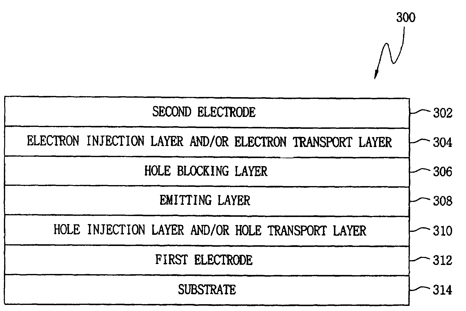
[0059]As shown in Example 8 of Table 1, it may be seen that an expected half life cycle of the device is increased nearly twice, as shown in FIG. 2, although a device having about 80 nm thick HTL (5% p-doping) without PEDOT that is a complete ionic material has a lower driving voltage and a slightly lower power efficiency compared to a device having a non-doped HIL containing structure shown in the Comparative Example.

[0060]TABLE 1Device structure: ITO / HIL(x nm) / HTL(y nm) / Red Dopant:CBP(8%, 22 nm) / Balq(5 nm) / Alq(20 nm) / LiF(8 nm) / Al(250 nm)PowerRedefficiencyluminanceHILHTLDopingat 300after 15thicknessthicknessratioHIL + HTLV at 300nitshours(Å)(Å)(%)(Å)nits(Lm / W)(%)EXAMPLE 1120020001220010.11.7657EXAMPLE 212008005200062.4358EXAMPLE 302000120008.41.6280EXAMPLE 4080018005.92.784EXAMPLE 56001400320006.72.371EXAMPLE 66001400320006.62.4371EXAMPLE 712002000522007.72.2552EXAMPLE 8080058005.62.887EXAMPLE 902000520007.81.7878EXAMPLE1200800120005.92.376410COMPARATIVE60020008006.043.3964EXAMPLE

[...


PUM

PropertyMeasurementUnit
Weightaaaaaaaaaa
Thicknessaaaaaaaaaa
Electric potential / voltageaaaaaaaaaa

Abstract

An organic electroluminescent device has an improved lifetime and may be driven at a low voltage. The organic electroluminescent device includes; a substrate; a first electrode to define a pixel region on the substrate; multiple organic film layers to perform light emission on the first electrode; and a second electrode laminated on the multiple organic film layers; wherein the multiple organic film layers include at least an emitting layer, and at least one of a hole injection layer and a hole transport layer. The at least one of the hole injection layer and the hole transport layer includes an electron acceptor material.

Description

CROSS-REFERENCE TO RELATED APPLICATIONS[0001]This application claims the benefit of Korean Patent Application No. 2003-6617, filed on Feb. 3, 2003, the disclosure of which is hereby incorporated herein by reference in its entirety.BACKGROUND OF THE INVENTION[0002]1. Field of the Invention[0003]The present invention relates to an organic electroluminescent device, more particularly, to an organic electroluminescent device capable of being driven at low voltage.[0004]2. Description of the Related Art[0005]An organic electroluminescent device (OELD) has advantages in that it is thin and lightweight. The components and processing are simple, high definition and a wide view angle are secured, a complete moving picture and high color purity are realized, and electrical characteristics appropriate a for mobile purpose are obtained by low power consumption and low voltage driving of a self-emitting type display using a phenomenon that light is generated as electrons are being connected to h...

Claims


Application Information

Patent Timeline
IPC IPC(8): H01L51/50H05B33/26C09K11/06H01L51/00H01L51/30H05B33/00H05B33/12H05B33/14H05B33/20
CPCH01L51/5052H01L51/005H01L51/0051H01L51/5096H01L51/5088Y10S428/917H10K85/60H10K85/611H10K50/155H10K50/165H10K50/17H10K50/18H05B33/26
Inventor SUH, MIN-CHUL
Owner SAMSUNG DISPLAY CO LTD
Why Eureka
Try Eureka