FeRAM having differential data
- Summary
- Abstract
- Description
- Claims
- Application Information
AI Technical Summary
Benefits of technology
Problems solved by technology
Method used
Image
Examples
first embodiment
[0030]FIG. 4 is a schematic diagram of a non-volatile ferroelectric memory device according to the present invention.
[0031] As shown in FIG. 4, the non-volatile ferroelectric memory device of the present invention includes a plurality of cell array block groups 10, a common data bus 20, a column selection control unit 30, and a sense amp unit 40.
[0032] The cell array block groups 10 includes two cell array blocks BLK (0,0), / BLK (0,0) which have the same structure and store opposite data (i.e. differential data). That is, two memory cells located at the same position in the cell array block BLK (0,0) and the cell array block / BLK (0,0) store differential data. Therefore, two memory cells (2T2C) are used to store one cell data, and the differential data stored in two unit cells are read from the cell array block group 10 or are written in the cell array block group 10 at the same time.
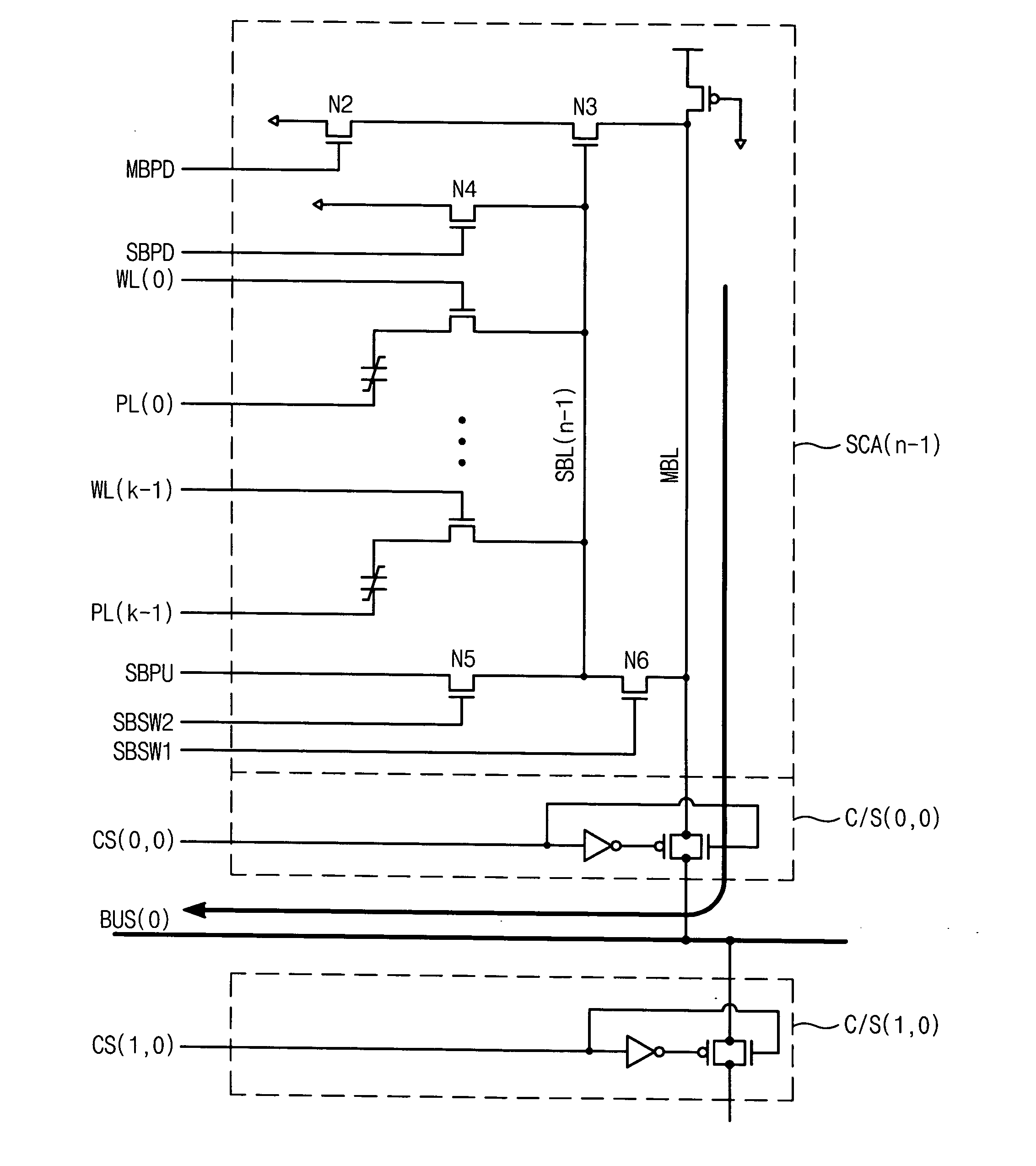
[0033] Each cell array block BLK (0,0), / BLK (0,0) has a hierarchy bit line architecture where a p...
second embodiment
[0059]FIG. 11 is a schematic diagram of a non-volatile ferroelectric memory device according to the present invention.
[0060] In the first embodiment, the respective cell array block group 10 comprises two adjacent cell array blocks. In the second embodiment, however, two cell array blocks BLK, / BLK in the respective cell array block group 10 are vertically symmetric with respect to the common data bus 20.
[0061] Therefore, the column selection control unit 40 in the second embodiment activates the column selection signals CS (0,0) and CS (1,0) at the same time.
[0062]FIG. 12 is a circuit diagram illustrating the 2T2C circuit structure of FIG. 11 for data sensing, and FIG. 13 is a timing diagram for describing the operation of FIG. 12.
[0063] When the word line WL (0) and the plate line PL (0) are activated, the data D1 or D0 in the unit cell C1 is applied to the sub bit line SBL. Likewise, the data / D1 or / D0 in the unit cell C2 is applied to the sub bit line / SBL. According to the ...
PUM
 Abstract
Description
Claims
Application Information


