Solder joint structure and method for soldering electronic components

a technology of electronic components and solder joints, which is applied in the direction of soldering apparatus, manufacturing tools, printed circuit non-printed electric components association, etc., can solve the problems of serious deformation of reliability of soldering, reduced joint strength, and inability to achieve required reliability of soldering, so as to achieve high reliability of lead-free soldering and reduce the effect of joint strength resulting from the interaction between copper and zin

Inactive Publication Date: 2005-06-16
ALPS ALPINE CO LTD
View PDF11 Cites 15 Cited by
  • Summary
  • Abstract
  • Description
  • Claims
  • Application Information

AI Technical Summary

Benefits of technology

[0015] According to this method, the first solder section is first formed on the first solder land, and a terminal of a heat-resistant electronic component chip is then mounted on the first solder land. When heated, highly reliable lead-free soldering can be performed. Soldering of thermolabile electronic components must be performed after the soldering of the electronic component chip. In this method, the first solder section is simultaneously formed on both the second solder lands and the first solder lands. Thus, the second solder section having a low melting point can be formed on the first solder section, i.e., the underlayer, on the second solder land. Thus, reliable fusion bonding between the lead terminal of the thermolabile electronic component and the second solder section can be achieved. In particular, a decrease in joint strength resulting from the interaction between copper and zinc can be prevented due to the presence of the first solder section, i.e., the underlayer. Reliable soldering of the thermolabile electronic components can be performed using the lead-free Sn—Zn solder without having to form costly gold plating layers. Moreover, no additional step of forming an underlayer for the second solder section is necessary since the first solder section is already formed

Problems solved by technology

However, a temperature cycling test in which the Sn—Zn solder material is applied on a patterned conductor containing copper, e.g., a copper foil, reveals that the joint strength decreases due to the interaction between copper and zinc and that the reliability of soldering is seriously degraded as a result.
In other words, required reliability cannot be achieved if soldering is performed by directly applying the Sn—Zn solder material on a solder land, i.e., a patterned copper foil, on a print circuit board.
However, since the nickel plating layer 3, which has poor solder wettability, must be coated with the gold plating layer 4, material cost is high, and the process requires extra steps.
Thus, increased cost has been a problem.

Method used


Image

  • Solder joint structure and method for soldering electronic components
  • Solder joint structure and method for soldering electronic components
  • Solder joint structure and method for soldering electronic components

Examples


Embodiment Construction

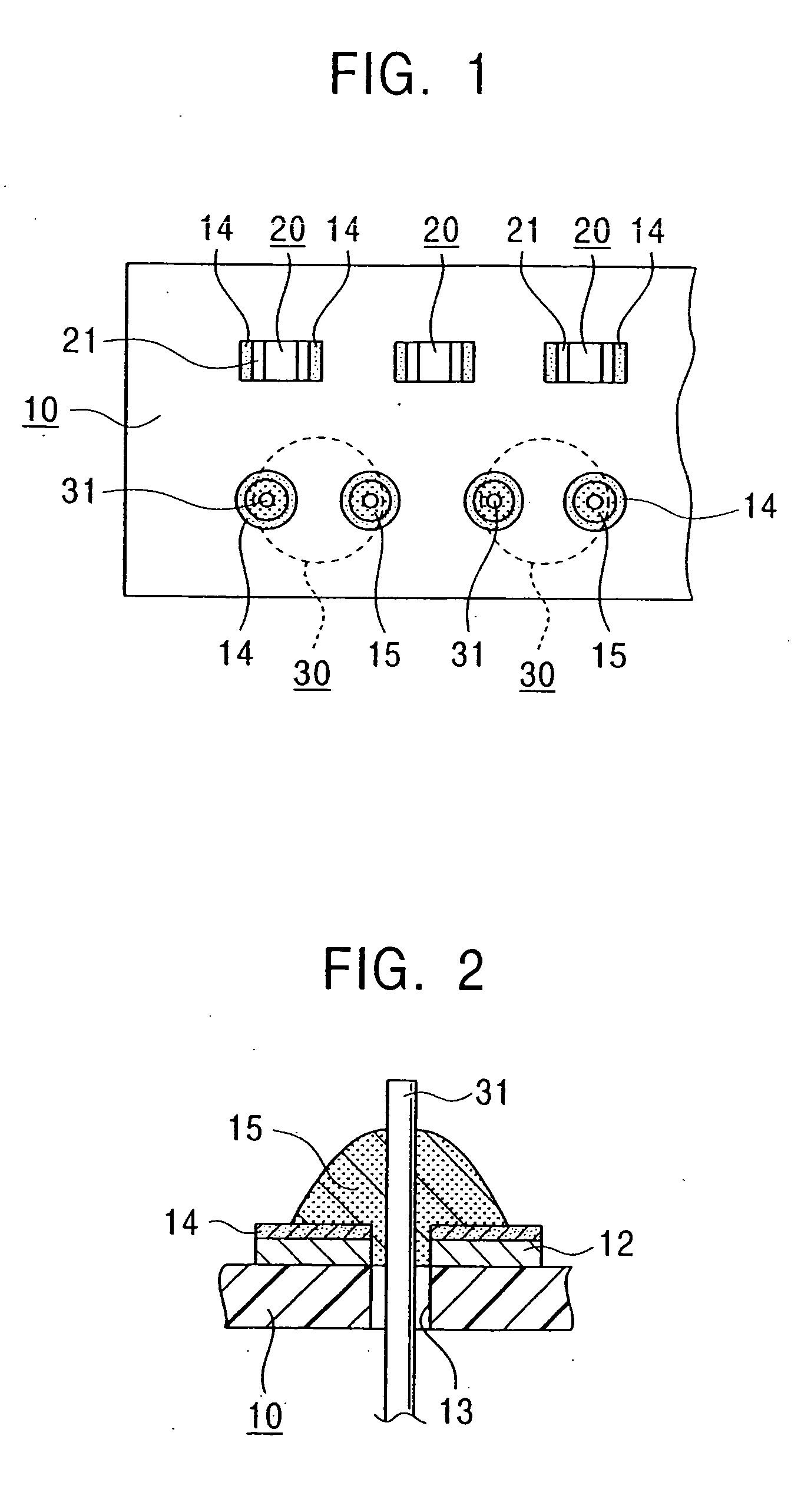
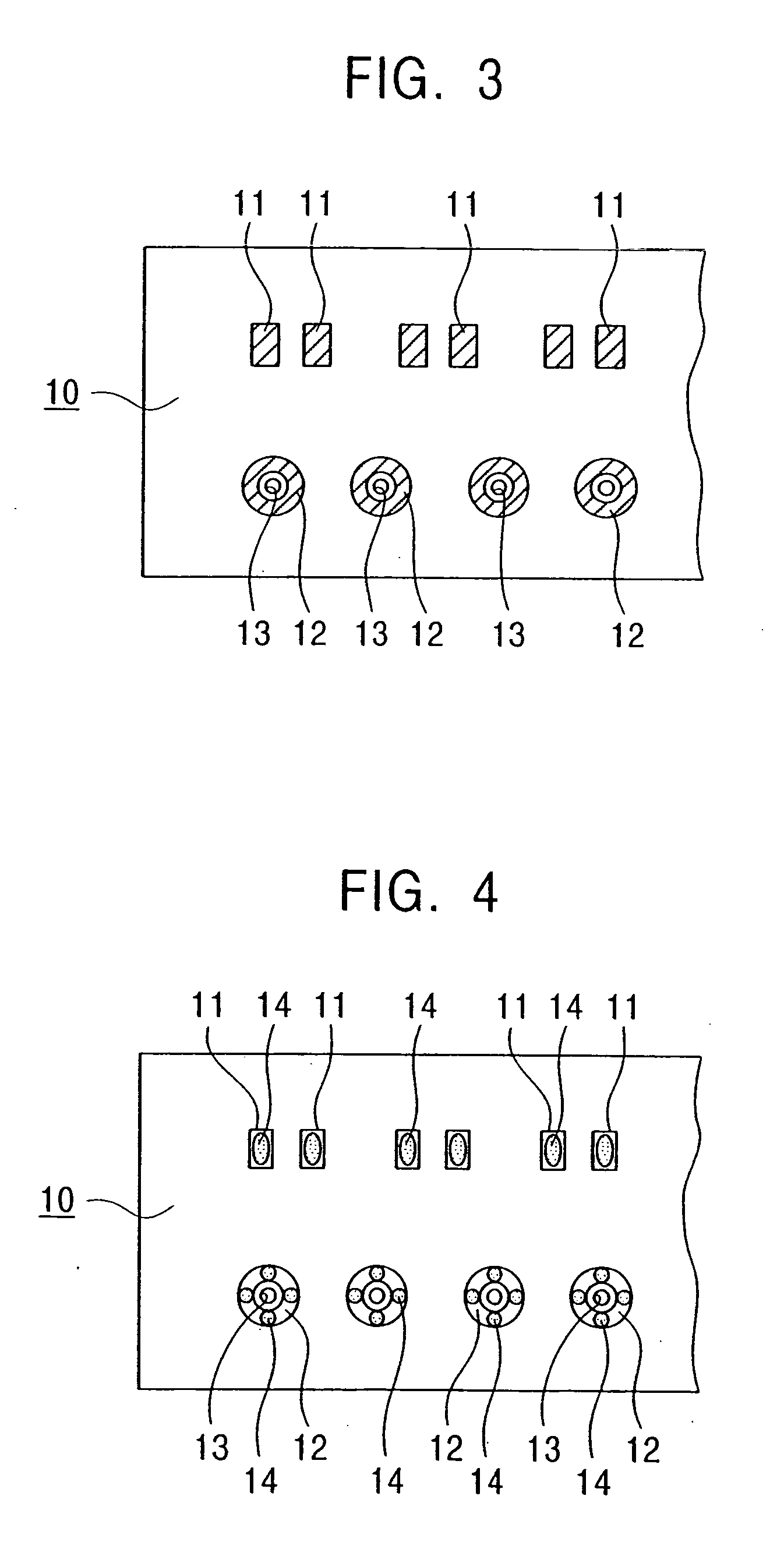
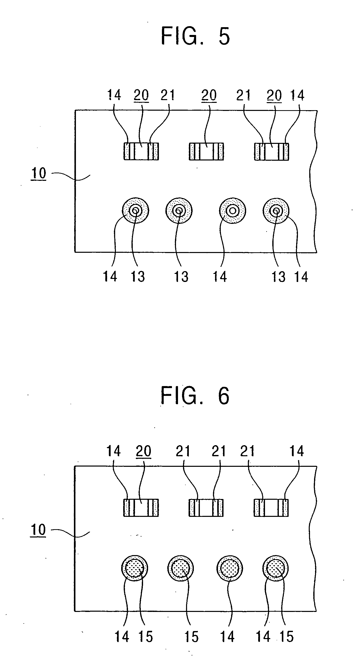
[0023] The preferred embodiments of the present invention will now be described with reference to the drawings. FIG. 1 shows a circuit board having various electronic components mounted thereon according to an embodiment of the present invention. FIG. 2 is a cross-sectional view of a solder joint structure for a lead terminal of a thermolabile electronic component. FIG. 3 shows lands on the circuit board. FIG. 4 shows the lands on the circuit board, which a Sn—Ag—Cu solder material is applied on the lands by printing. FIG. 5 shows the circuit board having electronic component chips mounted thereon. FIG. 6 shows the circuit board having second solder lands for lead terminals, in which a Sn—Zn solder material is applied on the solder lands by printing.

[0024] As shown in FIG. 3, first solder lands 11 for surface mounting and second solder lands 12 for use with lead terminals are formed on the same surface of a circuit board 10. The first solder lands 11 are patterned copper layers. A ...


PUM

PropertyMeasurementUnit
melting pointaaaaaaaaaa
temperaturesaaaaaaaaaa

Abstract

A method for soldering an electronic component is provided. A first solder land containing copper and a second solder land are formed on a surface of a circuit board. A first solder section composed of a Sn—Ag—Cu solder material is formed on each of the first and the second solder lands, and a terminal of an electronic component chip is mounted on the first solder land. The first solder land and the terminal are fusion-bonded. A second solder section composed of a Sn—Zn solder material is formed on the first solder section disposed on the second solder land. A lead terminal of another electronic component is inserted into a terminal hole formed near the second solder land; and the second solder section and the lead terminal are heated at a temperature lower than the temperature in step (d) to connect the lead terminal to the second solder section by fusion bonding.

Description

BACKGROUND OF THE INVENTION [0001] 1. Field of the Invention [0002] The present invention relates to a solder joint structure suitable for use in lead-free soldering of an electronic component having a low heat resistance and to a method of soldering electronic components. [0003] 2. Description of the Related Art [0004] In soldering terminals of various electronic components onto solder lands of print circuit boards, a Sn—Pb eutectic solder, e.g., 63Sn-37Pb solder, has been widely used. As the use of lead-free solder materials increases to avoid environmental pollution, various proposals of solder materials that meet the demand for lead-free soldering are made. Among such proposals, Sn—Ag—Cu solder materials are drawing much attention since they have superior thermal fatigue characteristics and creep property (e.g., Japanese Unexamined Patent Application Publication No. 2002-158438). Whereas Sn—Pb eutectic solder melts at 183° C., the melting point of Sn—Ag—Cu solder materials is hi...

Claims


Application Information

Patent Timeline
Patent Type & Authority Applications(United States)
IPC IPC(8): B23K1/00H05K1/18B23K35/26B23K101/36H05K1/09H05K3/34
CPCB23K1/0016B23K35/262H05K2203/047H05K3/3463H05K2201/10992H05K3/3447H05K1/18H05K3/34
Inventor KUBOKAWA, TERUYOSHIKOSAKA, KUNIONOMURA, TAKAFUMI
Owner ALPS ALPINE CO LTD
Why Eureka
Try Eureka