Semiconductor device, electronic circuit array substrate provided with the same and method of manufacturing the electronic circuit array substrate

a technology of semiconductors and electronic circuit arrays, which is applied in the direction of optics, transistors, instruments, etc., can solve the problems of difficult to manufacture liquid crystal display devices with little or no point-defect pixels at a good yield rate, point-defect pixels, electro-static destruction, etc., and achieve the effect of effectively suppressing the electrostatic destruction of semiconductors and improving the yield rate of electronic circuit array substrates

Active Publication Date: 2005-06-16
JAPAN DISPLAY CENTRAL CO LTD
View PDF3 Cites 9 Cited by
  • Summary
  • Abstract
  • Description
  • Claims
  • Application Information

AI Technical Summary

Benefits of technology

[0013] With this structure and / or method, when the front surface of interlayer film is washed with the fluids after the second aperture is made though it, electric discharges, which are substantially the same as the ones stored in the semiconductor layer, are carried into the lines though the second aperture. Thus, the electric potential at the lines is substantially equal to the one at the semiconductor layer. As a result, electrostatic destruction of the semiconductor is effectively suppressed so that the yield rate of an electronic circuit array substrate can be improved significantly.

Problems solved by technology

It is, however, extremely difficult to manufacture liquid crystal display devices with little or no point-defect pixels at a good yield rate.
One of the big causes of point-defect pixels is electro-static destruction in manufacturing an electronic circuit array substrate of a liquid crystal display device.
Abnormal characteristics of the thin-film transistors, for instance, may be caused by electro-static destructions in the case that an electronic circuit array substrate is washed after the formation of poly-crystalline silicon films patterned for thin-film transistors, a gate insulation film, scanning lines, auxiliary capacitor lines, an interlayer insulation film and contact holes in the interlayer and gate insulation films on the electronic circuit array substrate, i.e., before the formation of signal lines on the interlayer insulation film.

Method used


Image

  • Semiconductor device, electronic circuit array substrate provided with the same and method of manufacturing the electronic circuit array substrate
  • Semiconductor device, electronic circuit array substrate provided with the same and method of manufacturing the electronic circuit array substrate
  • Semiconductor device, electronic circuit array substrate provided with the same and method of manufacturing the electronic circuit array substrate

Examples


Embodiment Construction

[0021] Embodiments of the present invention will be described below with reference to the attached drawings. It should be noted that the present invention is not limited to the embodiments but covers their equivalents. Throughout the attached drawings, similar or same reference numerals show similar, equivalent or same components.

[0022] A liquid crystal display device of the first embodiment will be described below with reference to FIGS. 1-5.

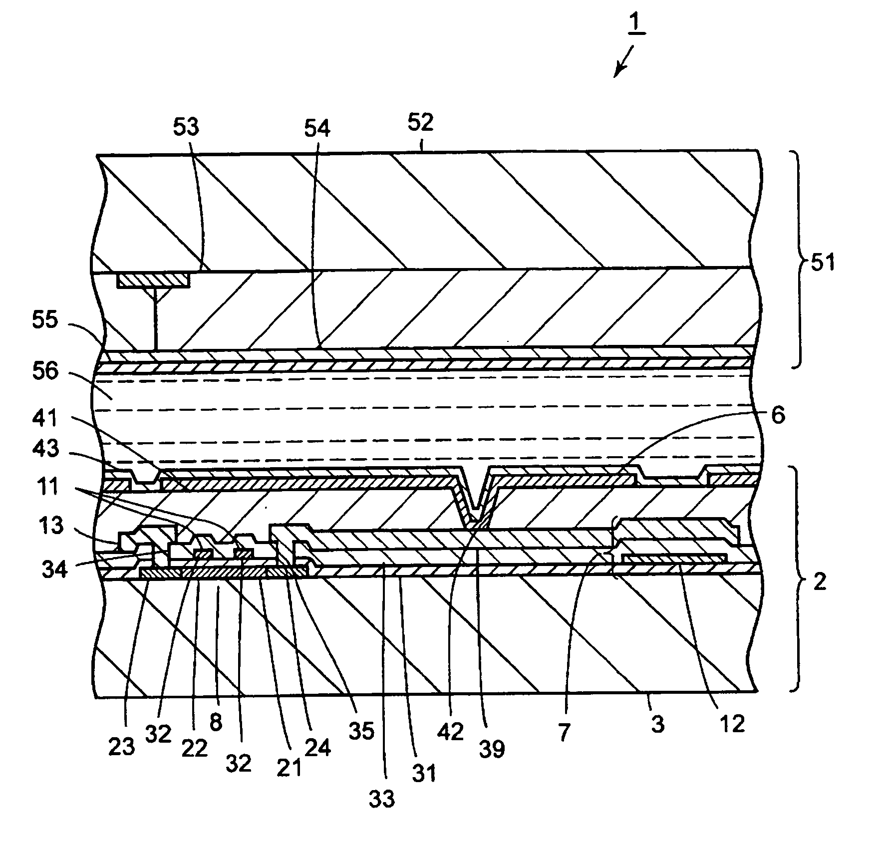
[0023] Liquid crystal display device 1 includes an electronic circuit array substrate such as thin-film transistor array substrate 2 in which top-gate-type thin-film transistors 8 are provided as shown in FIG. 5. Thin-film transistor array substrate 2 has a rectangular, optically transparent and electrically insulating substrate 3 such as # 1737 glass substrate manufactured by Corning Incorporated.

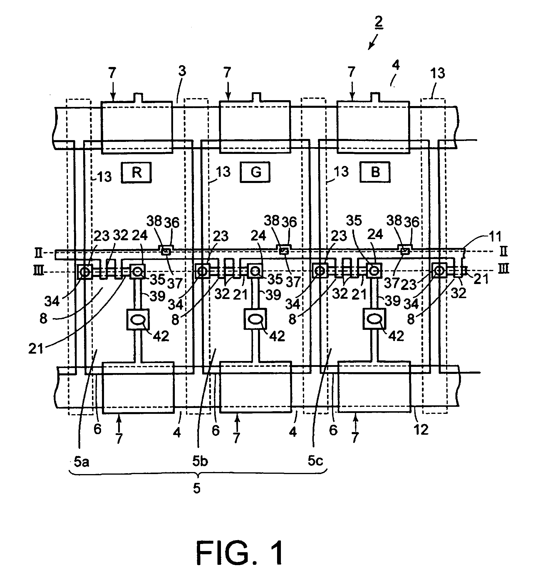
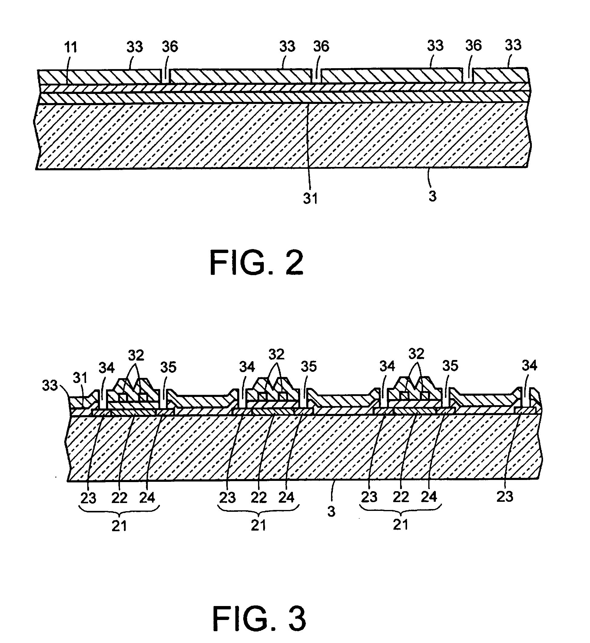
[0024] As shown in FIG. 4, glass substrate 3 contains display region 4 on its primary surface. Display region 4 is provided with a large number of...


PUM

PropertyMeasurementUnit
thickaaaaaaaaaa
thickaaaaaaaaaa
thickaaaaaaaaaa

Abstract

Dummy holes 36 are made for every one of display dot 5a, 5b and 5c at pixels 5 through interlayer film 33 up to gate electrode and scanning lines 11 before interlayer film 33 on glass substrate 3 is washed. When interlayer film 33 is washed, electric charges stored at semiconductor layer 21 are substantially the same in quantity as those stored at gate electrode and scanning lines 11 through dummy holes 36. Thus, electric potentials at gate electrode and scanning lines 11 are substantially equal in magnitude to those at semiconductor layer 21. This can suppress the occurrence of voltage differences imposed between gate electrode and scanning lines 11 and semiconductor layer 21.

Description

CROSS-REFERENCE TO RELATED APPLICATION [0001] This application is based upon and claims the benefit of priority from the prior Japanese Patent Application No. 2003-416676, filed on Dec. 15, 2003, the entire contents of which are incorporated in this application by reference.FIELD OF THE INVENTION [0002] This invention relates to a semiconductor device including a semiconductor layer arranged apart from an electrically conductive layer or line, an electronic circuit array substrate provided with the semiconductor device and a method of manufacturing the electronic circuit array substrate. BACKGROUND OF THE INVENTION [0003] Many liquid crystal display devices as flat panel display devices are provided with sandwich structures of electronic circuit array substrates, counter substrates and liquid crystal compositions as shown in Japanese Patent Publication 2000-187248 (particularly, see descriptions at pages 4-6 and FIGS. 1-3), for instance. The electronic circuit array substrates inclu...

Claims


Application Information

Patent Timeline
Patent Type & Authority Applications(United States)
IPC IPC(8): G02F1/13G02F1/1368G02F1/1362H01L21/3205H01L21/768H01L21/77H01L21/84H01L23/52H01L27/12H01L29/786H01L51/50
CPCH01L27/124G02F1/136227G02F1/13
Inventor KAWAMURA, TETSUYA
Owner JAPAN DISPLAY CENTRAL CO LTD
Why Eureka
Try Eureka