Local reduction of compliant thermally conductive material layer thickness on chips

a technology of thermally conductive material and chip, applied in the direction of electrical equipment, semiconductor devices, semiconductor/solid-state device details, etc., can solve the problems of local reduction of thermal resistance and so as to reduce the thermal resistance, reduce the temperature of the hot spot on the chip, and achieve adequate mechanical compliance

Inactive Publication Date: 2005-06-16
GLOBALFOUNDRIES INC
View PDF10 Cites 57 Cited by
  • Summary
  • Abstract
  • Description
  • Claims
  • Application Information

AI Technical Summary

Benefits of technology

[0014] The shortcomings of the prior art are overcome and additional advantages are provided through the provision of forming raised portions on the back surface of an integrated circuit in a pattern which corresponds to the hotter areas on the chip. This results in a projecting “mesa” structure on the back side of the chip so that after module assembly, the thickness of the compliant thermally conductive material layer is locally thinner over the “hot spots”. This results in a local reduction of the thermal resistance and hence a reduced temperature of the hot spot on the chip. By local reduction of the paste layer thickness, the allowable global paste layer thickness can be increased, or maintained at a thicker level, which reduces the likelihood of migration of the compliant thermally conductive material and the formation of voids between the chip and the heat sink or cold plate and insures that adequate mechanical compliance is provided between the chip and the heat sink or cold plate. Additionally, if individual pistons are used (as described in U.S. Pat. No. 6,214,647) to better control the compliant thermally conductive material layer thickness over each chip, additional small raised portions at the corners or along the edges of the chip can be formed to insure that the compliant thermally conductive material layer is uniform and that the piston, or heat sink, or cold plate, is not tilted relative to the chip surface.

Problems solved by technology

This results in a local reduction of the thermal resistance and hence a reduced temperature of the hot spot on the chip.

Method used


Image

  • Local reduction of compliant thermally conductive material layer thickness on chips
  • Local reduction of compliant thermally conductive material layer thickness on chips
  • Local reduction of compliant thermally conductive material layer thickness on chips

Examples


Embodiment Construction

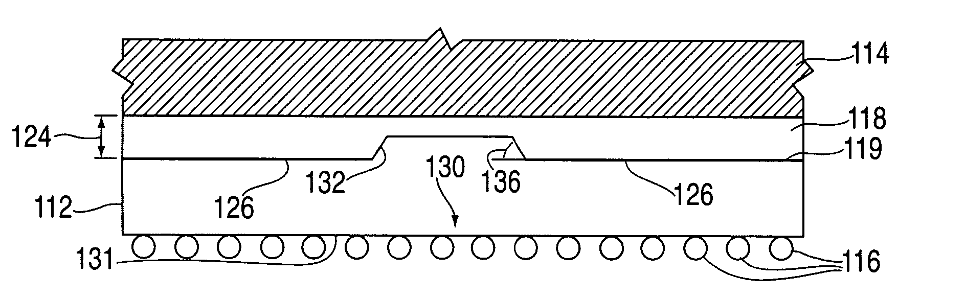
[0028] The present invention is directed at locally reducing the thickness of a compliant thermally conductive material in a region or regions aligned with high power density areas on a chip while avoiding migration of the material from behind the chip and the formation of voids.

[0029] As transistors are scaled down in size and as the operating frequency increases, the power density (W / cm2) of processor chips will continue to increase. For reliable long-term operation, it is necessary to remove the heat produced by a chip and keep the junction temperatures below about 105° C. Note that the acceptable junction temperature is a function of the technology used and the reliability requirements of the specific product.

[0030] Referring now to FIGS. 4(a) and 4(b), a semiconductor package structure 100 is illustrated. Structure 100 includes a chip 112 that is in thermal communication with a substrate 114 on one surface, while an opposite surface is operably connected to a C4 array 116 for...


PUM


Abstract

In an integrated circuit packaging structure, such as in an MCM or in a SCM, a compliant thermally conductive material is applied between a heat-generating integrated circuit chip and a substrate attached thereto. Raised regions are defined on the back side of the chip aligned to areas of a higher than average power density on the front active surface of the chip such that a thinner layer of the compliant thermally conductive material is disposed between the chip and the substrate in this area after assembly thereof resulting in a reduced “hot-spot” temperature on the chip. In an exemplary embodiment, the substrate includes one of a heat sink, cooling plate, thermal spreader, heat pipe, thermal hat, package lid, or other cooling member.

Description

CROSS-REFERENCE TO RELATED APPLICATIONS [0001] This application contains subject matter which is related to the subject matter of the following co-pending application, which is assigned to the same assignee as this application, International Business Machines Corporation of Armonk, N.Y. An application entitled “Improvement in chip cooling” having attorney docket number YOR920020329US1 filed on Dec. 27, 2002, is hereby incorporated herein by reference in its entirety. TECHNICAL FIELD [0002] This invention relates to cooling within integrated circuit (IC) packaging structures. More particularly, the present invention is directed to the cooling of integrated circuit chips using a relatively thick compliant thermally conductive material where there is a nonuniform power distribution on the integrated circuit. BACKGROUND OF THE INVENTION [0003] As heat is generated during the functioning of integrated circuit chips (ICs), the thermal resistance to the heat sink must be small so that the ...

Claims


Application Information

Patent Timeline
Patent Type & Authority Applications(United States)
IPC IPC(8): H01L23/34H01L21/50H01L21/56H01L23/10H01L23/12H01L23/36H01L23/367H01L23/373
CPCH01L23/367H01L2224/73204H01L2224/16H01L2224/73253H01L2924/01078H01L2924/10158H01L2924/15311H01L2924/01019H01L2924/10253H01L23/3737H01L2224/32245H01L2224/32225H01L2224/16227H01L2224/16225H01L2924/00H01L2924/181H01L2924/00012H01L23/36
Inventor COLGAN, EVAN G.FEGER, CLAUDISGOTH, GARY F.KATOPIS, GEORGE A.MAGERLEIN, JOHN H.SPROGIS, EDMUND J.
Owner GLOBALFOUNDRIES INC
Why Eureka
Try Eureka