Semiconductor device, semiconductor chip, method for manufacturing semiconductor device, and electronic apparatus

a semiconductor chip and semiconductor technology, applied in the direction of printed circuit assembling, printed circuit manufacturing, printed circuit aspects, etc., can solve the problems of further cost reduction, technical difficulties, etc., and achieve the effect of stable electronic connection, reliable electrical connection and reduced cos

Inactive Publication Date: 2005-06-16
SEIKO EPSON CORP
View PDF9 Cites 13 Cited by
  • Summary
  • Abstract
  • Description
  • Claims
  • Application Information

AI Technical Summary

Benefits of technology

[0022] In the semiconductor device manufactured by the above-described manufacturing method, since the conductive particles are securely sandwiched between the land on the wiring board and copper in the surface layer of the bump, a stable electronic connection may be maintained. Thus, according to the method for manufacturing a semiconductor device of the present invention, a semiconductor chip having a reliable electrical connection can be provided at a lower cost.
[0023] The above-described method for manufacturing a semiconductor device may further include the step of disposing a catalyst between the first conductive layer and the second conductive layer. The adhesion between the first conductive layer and the second conductive layer can be improved by properly selecting the catalyst.
[0024] In the above-described method for manufacturing a semiconductor device, at least one of the first conductive layer and the second conductive layer may be formed using an electroless plating. Since it is possible to form the bumps with a smaller variation of the height using electroless plating, a highly reliable semiconductor device can be provided at a lower cost.
[0025] An electronic apparatus according to the present invention includes the above-described semiconductor device, which can provide a highly reliable electronic device apparatus a lower cost.

Problems solved by technology

This technique, however, has a problem.
Thus, a further cost reduction cannot be achieved since it is necessary to form a gold layer having a sufficient thickness.

Method used


Image

  • Semiconductor device, semiconductor chip, method for manufacturing semiconductor device, and electronic apparatus
  • Semiconductor device, semiconductor chip, method for manufacturing semiconductor device, and electronic apparatus
  • Semiconductor device, semiconductor chip, method for manufacturing semiconductor device, and electronic apparatus

Examples


first embodiment

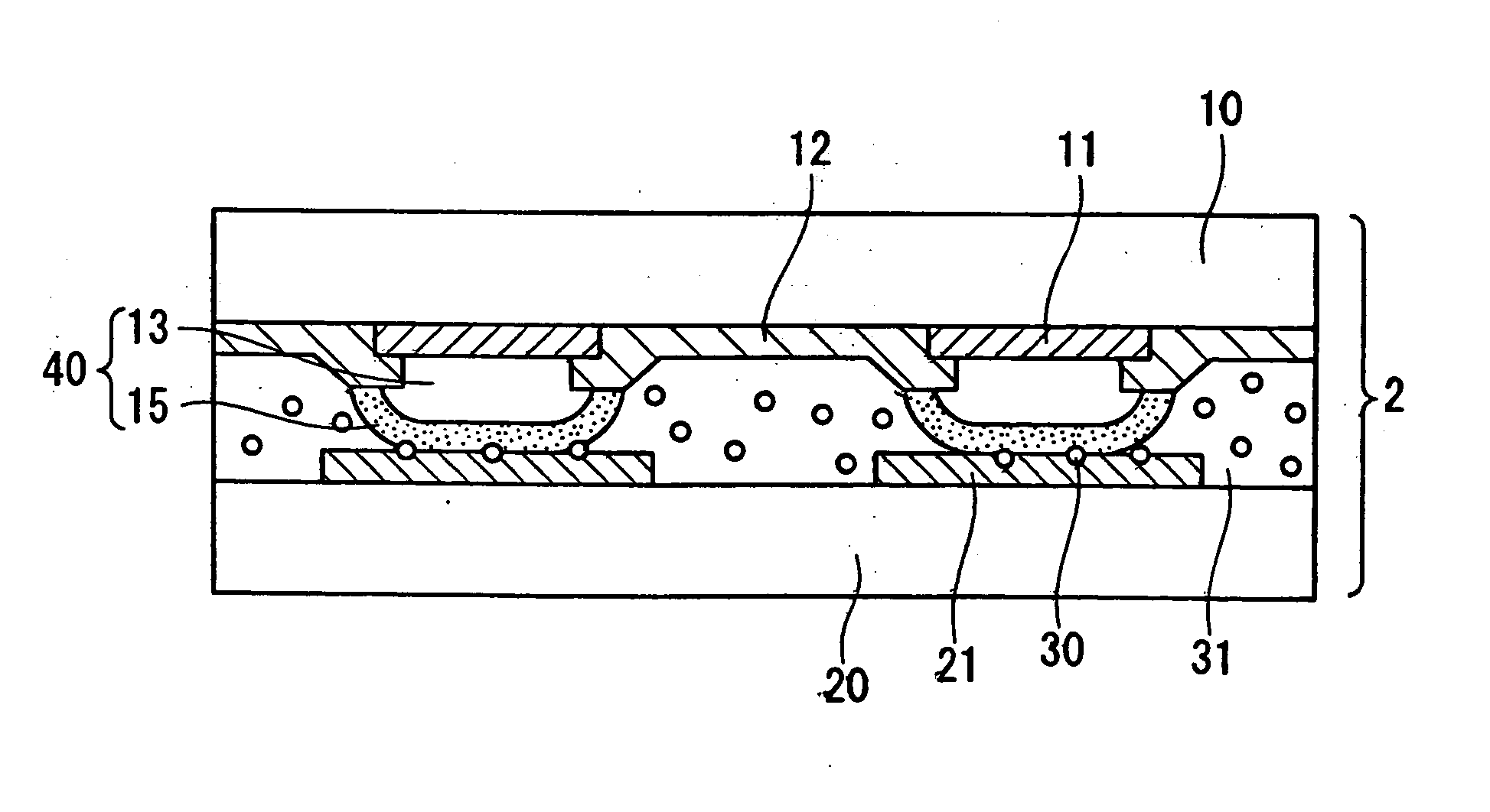
[0033]FIG. 2 is a schematic cross-sectional view which schematically illustrates a semiconductor device according to a first embodiment.

[0034] A semiconductor device 2 includes a semiconductor chip 1, a wiring board 20 provided with a plurality of lands 21, and an anisotropic conductive resin layer 31 which is dispersed with conductive particles 30.

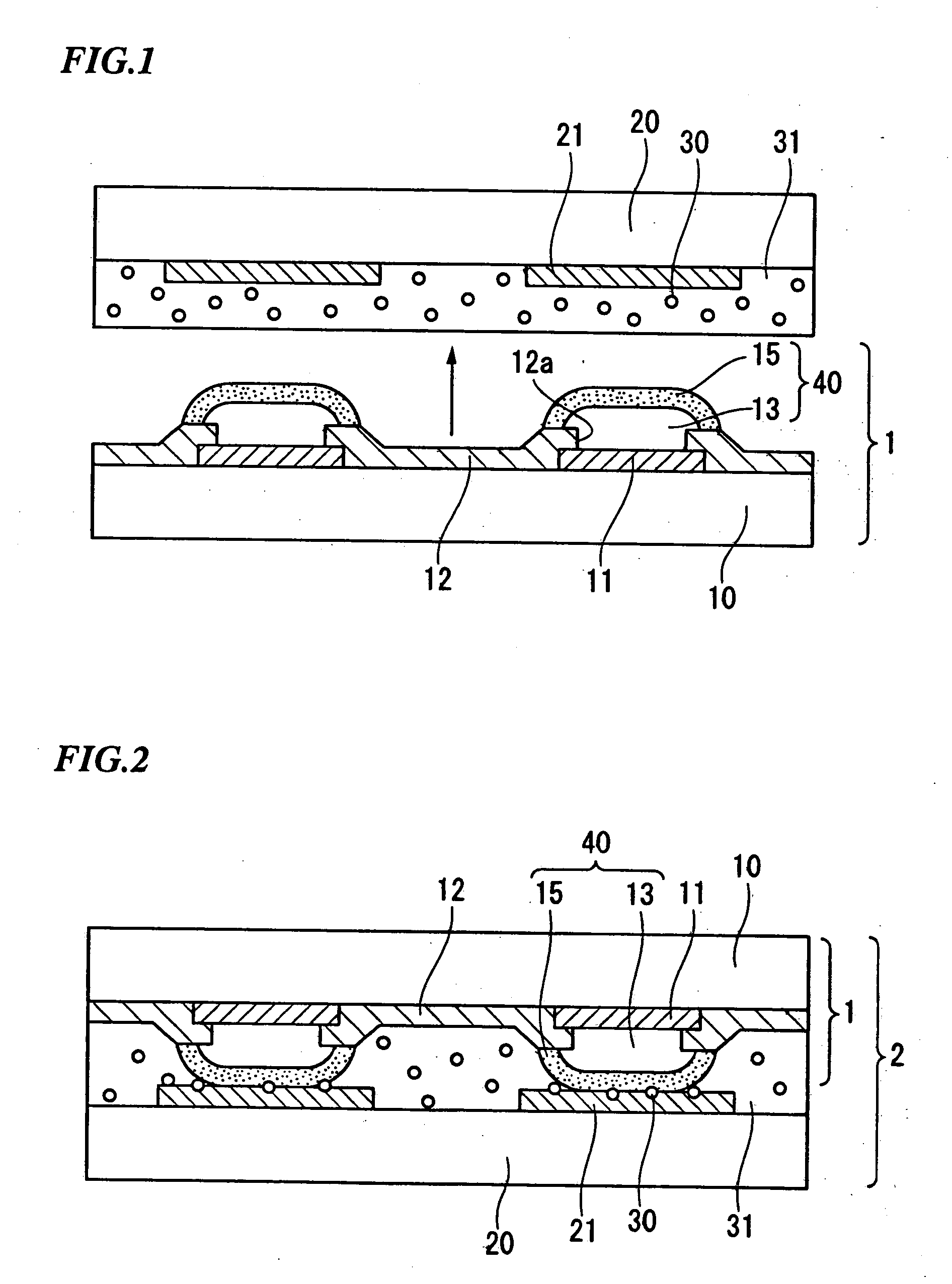
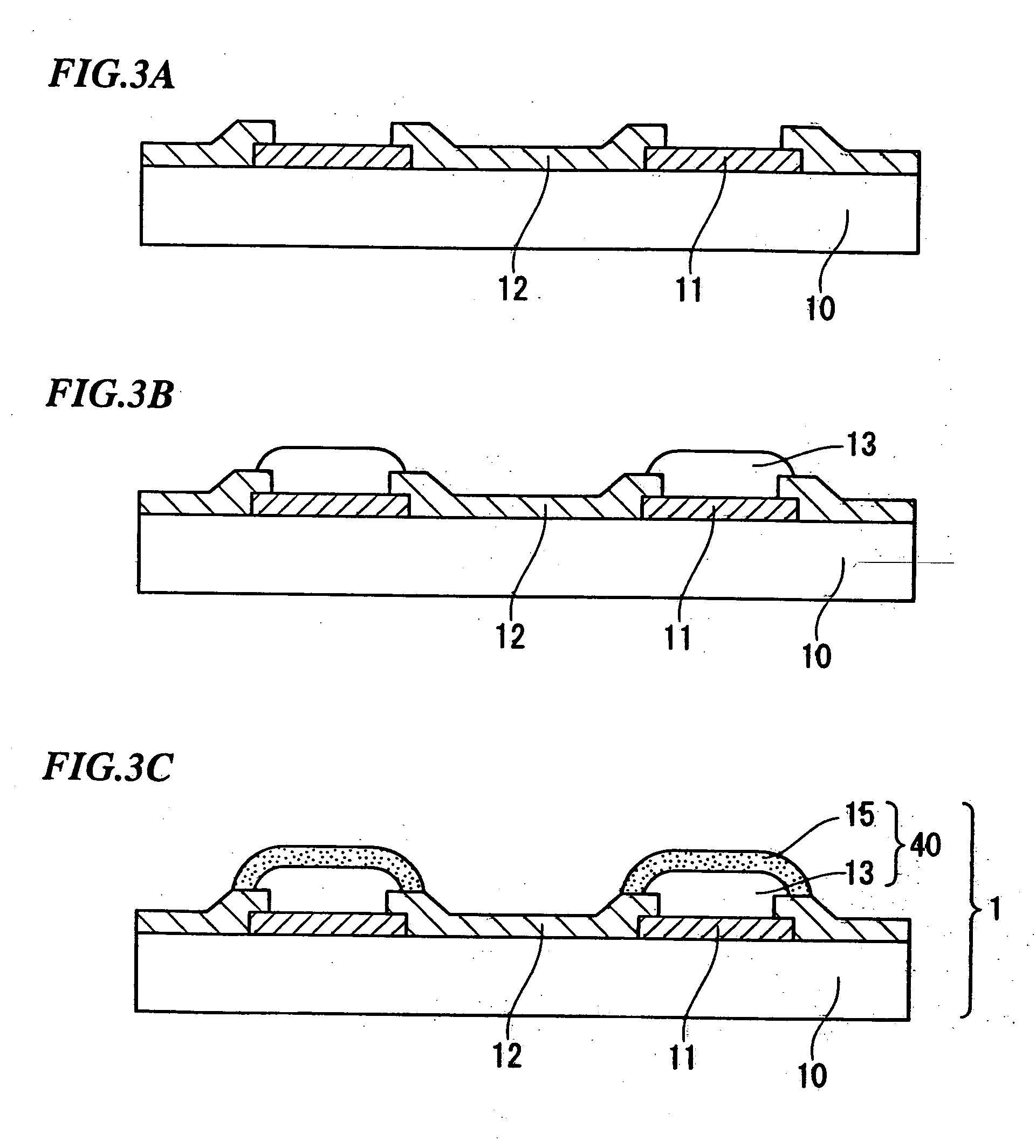
[0035]FIG. 1 is a schematic cross-sectional view which schematically illustrates a semiconductor chip according to the first embodiment.

[0036] The semiconductor chip 1 includes a plurality of outer-connection electrodes 11 provided on one side of a substrate 10 made of, for example, silicon, and bumps 40 having a first conductive layer 13 and a second conductive layer 15 which are stacked together. The first conductive layer 13 is made of, for example, nickel and has a thickness ranging from 10 μm to 25 μm, preferably about 15 μm. The second conductive layer 15 is made of copper and has a thickness of about 5 μm. The outer-connection e...

second embodiment

[0057] Next, a second embodiment of a semiconductor chip according to the present invention will be described. FIG. 4 is a schematic cross-sectional view schematically illustrating the second embodiment of the semiconductor chip, which corresponds to the first embodiment shown in FIG. 1. A semiconductor chip 3 of the second embodiment includes a bump 40 which includes a first conductive layer 13 and a second conductive layer 15, and a bump 40 is provided on each of a plurality of outer-connection electrodes 11 disposed on one side of a substrate 10 which is made of silicon. The second embodiment differs from the first embodiment in that the first conductive layer 13 is provided in an opening 12a provided in a passivation film 12, and the first conductive layer 13 has a thickness equal to or smaller than the thickness of the passivation film 12. In other words, the first conductive layer 13 is provided only in the opening 12a of the passivation film 12. The first conductive layer 13 ...

third embodiment

[0061]FIG. 5 is a cross-sectional view of a semiconductor device according to a third embodiment of the present invention. As shown in FIG. 5, a third conductive layer 13′ which is softer than the first conductive layer 13 may be provided between the first conductive layer 13 and the second conductive layer 15. In this embodiment, the first conductive layer 13 is made of nickel (Ni) and the third conductive layer 13′ is made from gold (Au) which is a softer metal than nickel. The third conductive layer 13′ may reduce damage (silicon cracks) to the substrate 10 which is located below the outer-connection electrodes 11 during bonding. The third conductive member 13′ made of gold may prevent oxidation of the first conductive layer 13 and the like. The third conductive member 13′ also serves as a catalyst in the above-described embodiments.

[0062] In the embodiments mentioned above, the thickness of an outer-connection electrode 11 which is provided within an opening 12a of a passivatio...


PUM


Abstract

A semiconductor device including: a semiconductor chip including a substrate, an outer-connection electrode, and a bump, wherein the bump has a first conductive layer and a second conductive layer provided on the first conductive layer, and the second conductive layer is made of copper; a wiring board having a land; and an insulating material dispersed with conductive particles, wherein the conductive particles connect between the bump and the land, wherein an electrical connection is established by the conductive particles having penetrated to both the second conductive layer and the land.

Description

BACKGROUND OF THE INVENTION [0001] 1. Field of the Invention [0002] The present invention relates to a semiconductor device, to a semiconductor chip, to a method for manufacturing a semiconductor device, and to an electronic apparatus, and particularly to a semiconductor chip which is tailored to flip-chip mounting technique. [0003] Priority is claimed on Japanese Patent Application No. 2003-407386, filed Dec. 5, 2003, and Japanese Patent Application No. 2004-305519, filed Oct. 20, 2004, the contents of which are incorporated herein by reference. [0004] 2. Description of Related Art [0005] At present, there is a strong demand to reduce the size, width, and weight, and manufacturing cost of mobile electronic apparatuses, such as portable phones and notebook-type personal computers. In order to meet such a demand, higher integration of semiconductor chips used in various electronic apparatuses has been considered, and various semiconductor mounting techniques have been researched and ...

Claims


Application Information

Patent Timeline
Patent Type & Authority Applications(United States)
IPC IPC(8): H01L21/00H01L21/28H01L21/60H01L23/02H01L23/12H01L23/48H01L23/498H01L29/40H01R11/01H05K3/32
CPCH01L23/49811H01L2224/83851H01L24/12H01L24/16H01L24/28H01L24/83H01L2224/13099H01L2224/73204H01L2924/01005H01L2924/01013H01L2924/01029H01L2924/0103H01L2924/01033H01L2924/01046H01L2924/01047H01L2924/01078H01L2924/01079H01L2924/0781H01L2924/14H05K3/323H05K2201/023H05K2201/10674H01L2224/2919H01L2924/01006H01L2924/0665H01L24/11H01L2224/83205H01L2224/81192H01L2224/81191H01L2924/00H01L2924/3512H01L2924/15787H01L2224/05567H01L2224/05573H01L2224/05624H01L2224/05647H01L2224/05022H01L24/29H01L24/32H01L24/13H01L2924/00014H01L23/12H01L21/60
Inventor IMAI, HIDEO
Owner SEIKO EPSON CORP
Why Eureka
Try Eureka