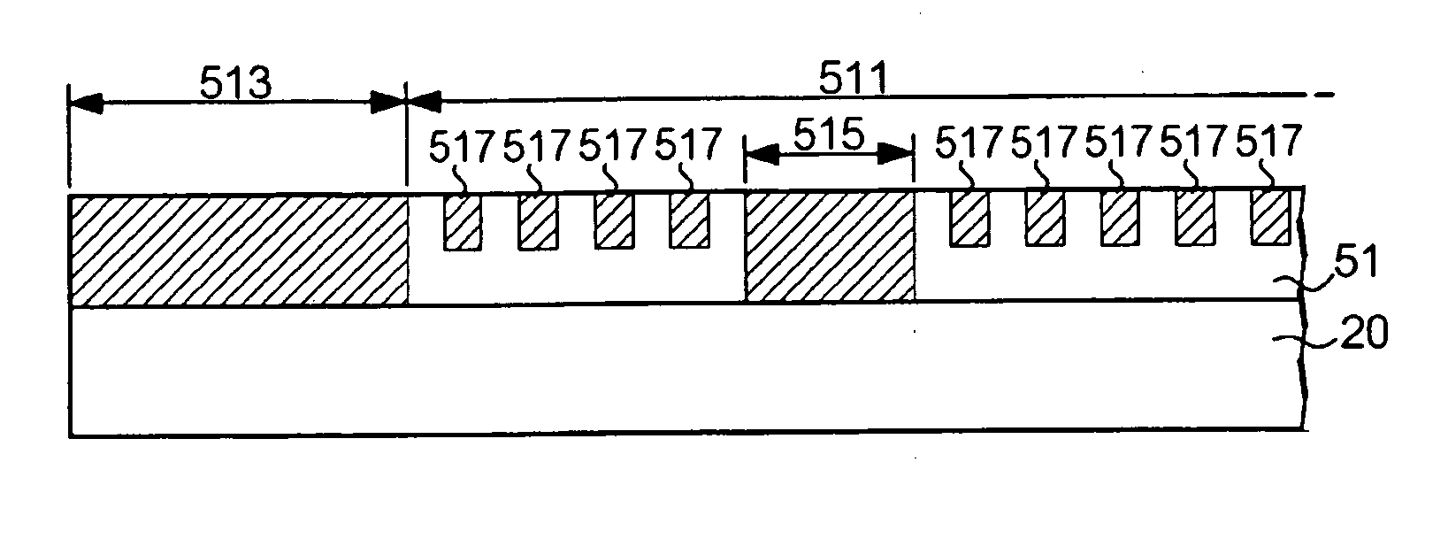
[0011] According to another aspect of the invention, the
photomask includes a
peripheral transmissive portion in contact with the entire edge or part of the edge of each dot region. The
peripheral transmissive portion transmits light at substantially the same
transmittance as that of the transmissive portion in the first region. With such a structure, of the light that travels from the
light source toward the film, the light that has passed through the
peripheral transmissive portion is diffracted around the edge of each dot region, and the diffracted light is intensified at the surface of the film. Therefore, in addition to the region of the film which is irradiated with the light that has passed through the semitransmissive portion, the region irradiated with the diffracted light that has passed through the peripheral transmissive portion is also photodecomposed and so, a fine recess is formed in each of the regions of the
ground layer formed by developing the film, which correspond to the dot regions. Forming a thin-film reflecting layer on the roughened surface of the
ground layer offers a preferable light-
scattering effect as compared with a case in which the reflecting layer is formed on a roughened surface of which the tops of the projections or the bottoms of the recesses are flat.
[0012] The photomask may be constructed such that the peripheral transmissive portion is in contact with the entire edge of each dot region or, alternatively, the peripheral transmissive portion that transmits light at substantially the same light
transmittance as that of the transmissive portion is interposed between the dot region and the semitransmissive portion. Such a structure ensures the amount of light that is diffracted at the edge of the dot region into the film, thus forming a recess with a prescribed depth at the top of the projection of the roughened surface. According to the embodiments, the amount of light that has passed through the peripheral transmissive portion and is diffracted at the edge of the dot region (in other words, the depth of the recess formed at the top of the projection on the roughened surface) is adjusted according to the length of the contact portion with the edge of the dot region in the peripheral transmissive portion. Accordingly, it is preferable to select the structure of the peripheral transmissive portion according to the depth of the recess to be formed on the top of the projection on the roughened surface. Specifically, the invention may adopt a structure in which the peripheral transmissive portion is disposed in contact with the entire edge of the dot region or a structure in which the peripheral transmissive portion is disposed in contact with part of the edge of the dot region. The former structure can increase the amount of diffracted light at the edge of the light-shielding portion as compared with the latter structure, thereby allowing a deep recess to be formed at the top of the projection on the roughened surface. In other words, the latter structure allows the depth of the recess formed on the top of the projection on the roughened surface to be reduced.
[0013] On the other hand, a photomask used for forming a roughened surface (a roughened surface in which regions of the film which correspond to the dot regions have projections) by removing a region other than the dot regions of the process region of a film made of a negative photosensitive material includes a first region having a light-shielding portion that shields light traveling toward the periphery of the process region and a second region including a plurality of dot regions each having a transmissive portion that transmits light traveling toward the process region and a semitransmissive portion that transmits the light traveling toward the process region in a region other than the dot regions, the semitransmissive portion transmitting the light at a lower transmittance than that of the transmissive portion. A specific example of the structure will be described hereinafter as a third embodiment. A photomask used for forming a roughened surface (a roughened surface in which regions of the film which correspond to the dot regions have recesses) by removing the dot regions of the process region of a film made of a negative photosensitive material includes a first region having a light-shielding portion that shields light traveling toward the periphery of the process region; and a second region including a plurality of dot regions each having a semitransmissive portion that transmits light traveling toward the process region at a lower transmittance than that of the transmissive portion and a transmissive portion that transmits the light traveling toward the process region in a region other than the dot regions. A specific example of the structure will be described hereinafter as a fourth embodiment. The use of the photomask facilitates forming the
ground layer of the reflecting layer having a preferable light-
scattering effect, as with the above-described photomask for exposing the positive photosensitive material.
[0015] The semitransmissive portion may have any specific structure only if it has lower light transmittance than the transmissive portion. For example, an extremely thin light-shielding film absorbs or reflects part of light that is applied thereto and transmits other part of the light. Such a light-shielding thin film may be used as the semitransmissive portion. Alternatively, a sheet-like arrangement of multiple fine light-shielding portions and multiple fine transmissive portions may be used as the semitransmissive portion. Such a structure also allows part of the light from the
light source to be shielded by the fine light-shielding portions and other part to be passed through the fine transmissive portions. Although the fine light-shielding portions and the fine transmissive portions may be disposed in any arrangements, it is preferable to use a semitransmissive portion in which the fine light-shielding portions and the fine transmissive portions are arranged alternately in a first direction and a second direction (in checkered pattern), in viewpoint of uniformizing the amount of light that passes through the semitransmissive portion into the film in the plane of the semitransmissive portion. With such a structure, in order to prevent the mutual interference of the light that has passed through the fine transmissive portions and is diffracted at the edge of the fine light-shielding portions, it is preferable to set the side of each of the fine light-shielding portions and the fine transmissive portions at 2 μm or less and, more preferably, at 1.5 μm or less. Another aspect of the invention, the semitransmissive portion may have a structure in which the fine light-shielding portions and the fine transmissive portions extending in a first direction are disposed alternately in a second direction orthogonal to the first direction (stripe pattern). Also with such a structure, in order to prevent the mutual interference of the light that has passed through the fine transmissive portions and is diffracted at the edge of the fine light-shielding portions, it is preferable to set the width of each of the fine light-shielding portions and the fine transmissive portions at 2 μm or less and, more preferably, at 1.5 μm or less.
[0017] Preferably, the photomask according to the invention has a dot region (light-shielding portion) shaped like a substantially oblate figure in planar shape or a substantially polygon in planar shape whose circumscribed circle is oblate. The “oblate figure” in the invention is an
ellipse other than a perfect circle and includes various shapes including a shape having a rectangle or square to the opposite sides of which a semicircle with the
diameter thereof is added (refer to FIG. 24), in addition to an
ellipse. When a photomask in which the planar shape of each dot region is a perfect circle or a polygon whose circumscribed circle is a perfect circle is used for
exposure (hereinafter, referred to as a comparative example), diffracted light around the entire edge of the dot region is concentrated in a small region of the film (in the center of the film which overlaps with the dot region) at substantially the same phase, thus intensifying each other. In that case, intense light is applied to the portion in which the diffracted light is concentrated, or the region of the film which is to be the top of the projection of the roughened surface, so that a roughened surface formed by the following development will have a deep recess at the top of the projection. If the top of the projection is a flat surface having no recess,
mirror reflection will occur at the surface of the reflecting layer which covers the top of the projection, having limits in offering a preferable light-
scattering effect. Accordingly, in order to offer a preferable light-scattering effect, it is preferable to provide a recess at the top of the projection on the roughened surface. However, test results by the inventor have shown that the use of the photomask according to the comparative example excessively increases the recess of the top of the projection, reducing the light-scattering effect.
[0024] The electrooptic device substrate according to the invention includes a ground layer having a plurality of projections on the surface, the projections being substantially oblate in planar shape and each having a recess on the top thereof; and a light-reflective reflecting layer disposed on the surface of the ground layer having the plurality of projections. Since the electrooptic device substrate has a recess at the top of each projection on the roughened surface of the ground layer, the ratio of the flat portion on the surface of the reflecting layer is small, thus offering a preferable light-scattering effect. The ground layer of the electrooptic device substrate can be formed by developing the film after
exposure using the photomask according to the invention.


