Method for etching of a silicon substrate and etching apparatus

a technology of etching apparatus and silicon substrate, which is applied in the direction of electrical apparatus, decorative surface effects, decorative arts, etc., can solve the problems of uneven wall surfaces, poor processing precision, and new wall surfaces formed by etching without protective films, etc., and achieve excellent perpendicularity and sufficient smoothness without reducing etching speed

Active Publication Date: 2005-06-16
SUMITOMO PRECISION PROD CO LTD
View PDF3 Cites 19 Cited by
  • Summary
  • Abstract
  • Description
  • Claims
  • Application Information

AI Technical Summary

Benefits of technology

[0015] An object of the present invention is to provide an etching method and etching apparatus for a silicon substrate which results in etching

Problems solved by technology

However, with the above etching method, there were the following problems.
As a result, the new wall surfaces formed by etching do not have a protective film.
As a result, the wall surfaces have an undulating surface in the vertical direction, and the processing precision is poor.
This unevenness of the wall surfaces becomes an o

Method used


Image

  • Method for etching of a silicon substrate and etching apparatus
  • Method for etching of a silicon substrate and etching apparatus
  • Method for etching of a silicon substrate and etching apparatus

Examples


experiment 1

1. Experiment 1

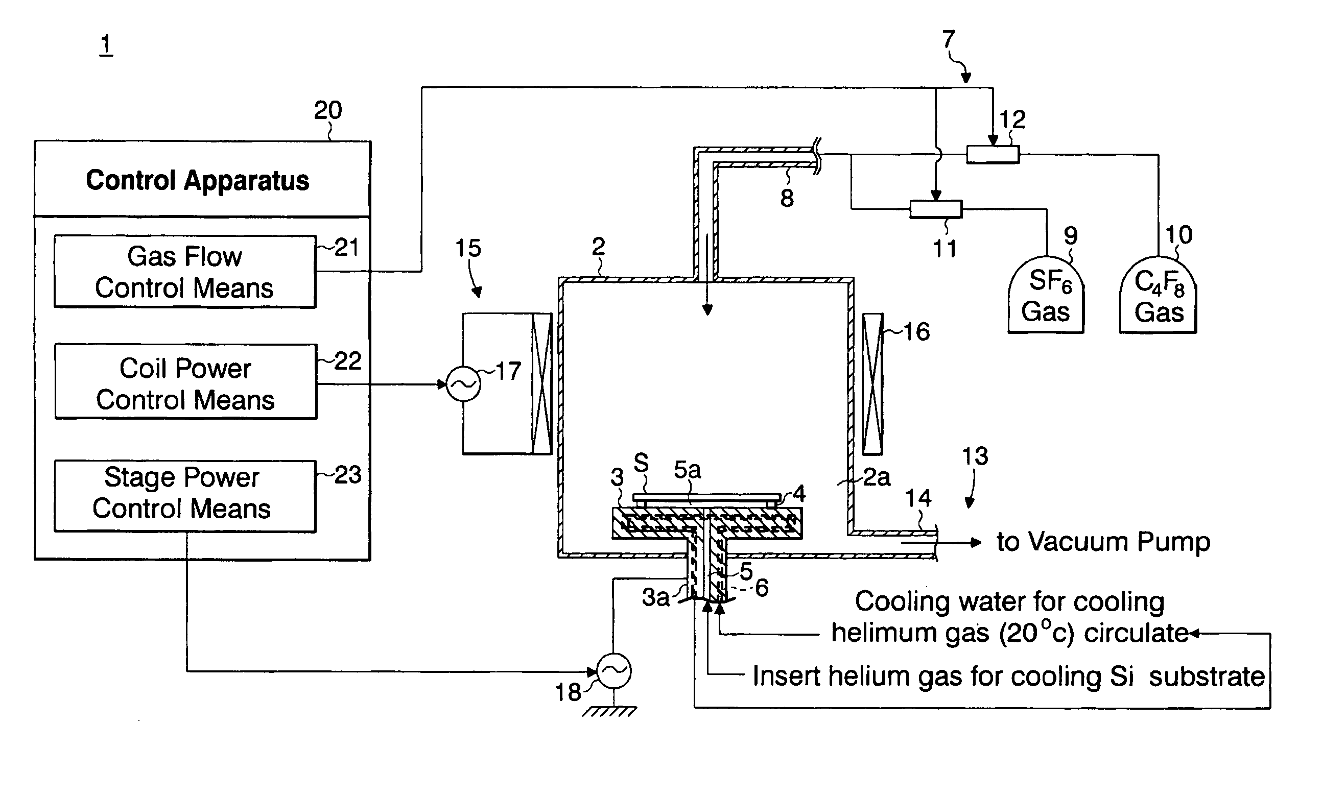
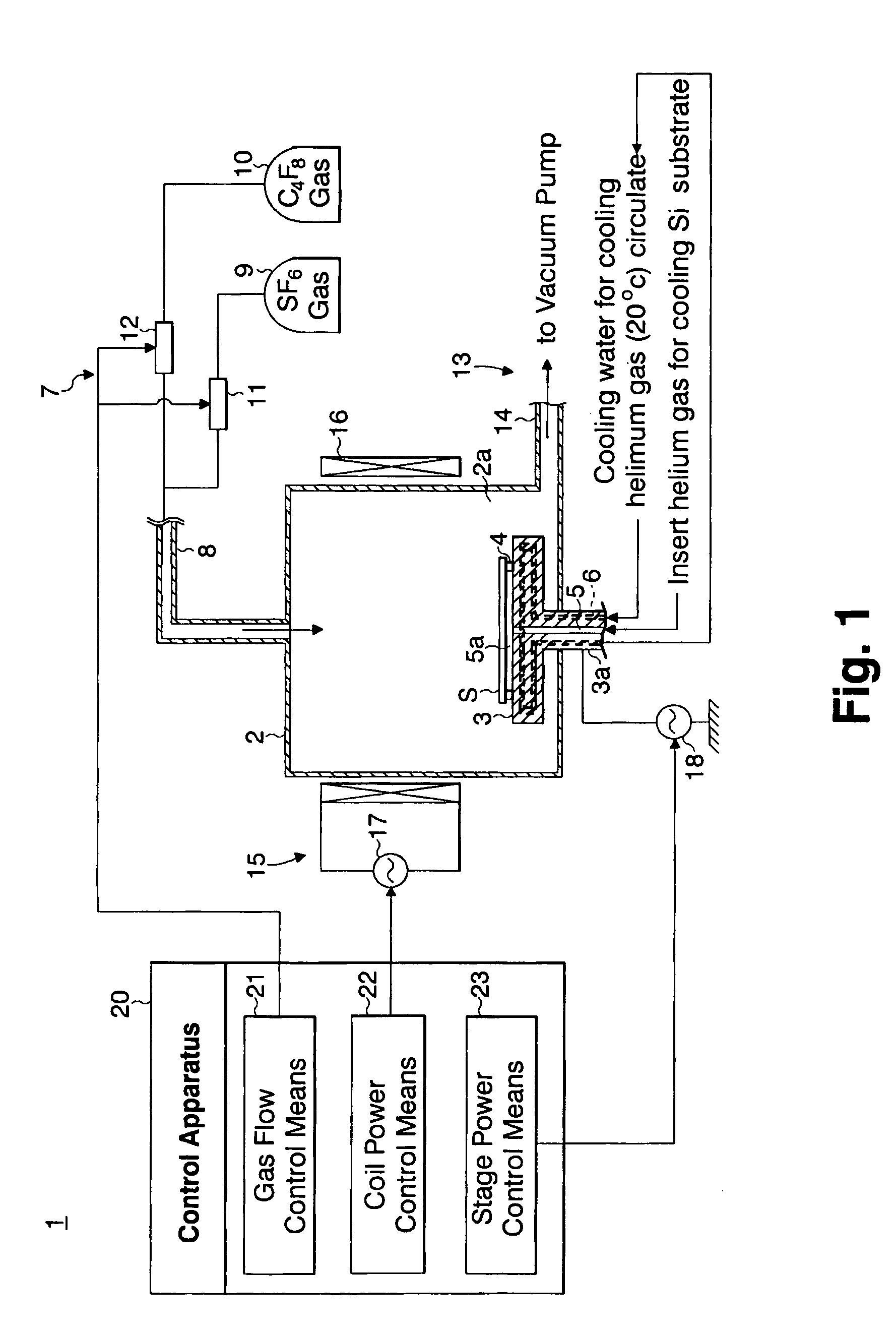
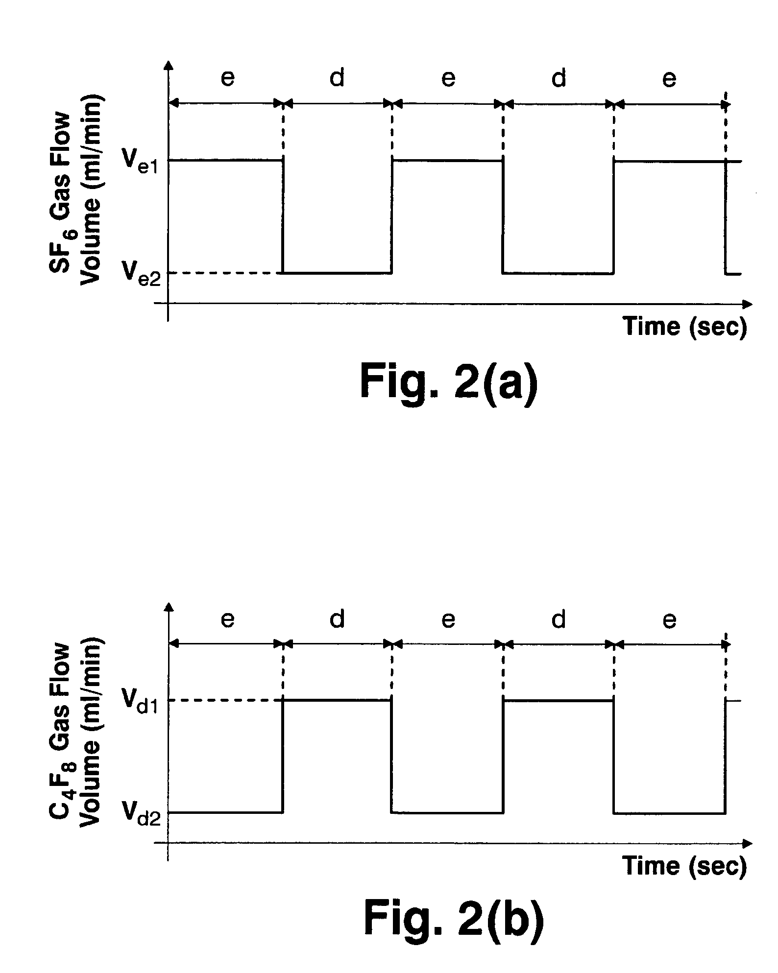
[0075] For the etching gas, SF6 gas was used, and for the protective film formation gas, C4F8 gas was used. For the high frequency power applied to coil 16, Wo1 was 2200 W, and Wo2 was 1500 W. For the high frequency power applied to stage 3, Wp1 was 40 W, Wp2 was 20 W. Flow rate Ve1 of SF6 gas during step e was 450 ml / min, and flow rate Vd1 of C4F8 gas during step d was 150 ml / min. During step d, flow rate Ve2 for SF6 gas changed to 0 ml / min, 3 ml / min, 4.5 ml / min, 7.5 ml / min, 15 ml / min. Furthermore, during step e, flow rate Vd2 of C4F8 gas changed to 0 ml / min, 22.5 ml / min, 31.5 ml / min, 54 ml / min, 90 ml / min, 135 ml / min. The silicon substrate was etched under these conditions, and a hole 31 as shown in FIG. 3 was formed on the silicon substrate.

[0076] The processing time for step e was 8.5 seconds and the processing time for step d was 3 seconds. Steps e and d were implemented repeatedly for 15 minutes. In addition, the pressure inside etching chamber 2 was 4.0 Pa in s...

experiment 2

2. Experiment 2

[0082] SF6 gas was used again as etching gas, and C4F8 gas was used as protective film formation gas. For the high frequency power applied to coil 16, Wo1 was 900 W and Wo2 was 800 W. For the high frequency power applied to stage 3, Wp1 was 25 W and Wp2 was 5 W. Flow rate Ve1 of SF6 gas during step e was 200 ml / min, and flow rate Vd1 of C4F8 gas during step d was 60 ml / min. During step d, flow rate Ve2 for SF6 gas changed to 0 ml / min, 1.2 ml / min, 1.8 ml / min, 3 ml / min, 6 ml / min. Furthermore, during step e, flow rate Vd2 of C4F8 gas changed to 0 ml / min, 10 ml / min, 14 ml / min, 24 ml / min, 40 ml / min. The silicon substrate was etched under these conditions, and a hole 31 as shown in FIG. 3 was formed on the silicon substrate.

[0083] The processing time for step e was 15 seconds and the processing time for step d was 7 seconds. Steps e and d were implemented repeatedly for 30 minutes. In addition, the pressure inside etching chamber 2 was 2.5 Pa in step e and 0.8 Pa in step d...


PUM

PropertyMeasurementUnit
Bias potentialaaaaaaaaaa
Poweraaaaaaaaaa
Volumeaaaaaaaaaa

Abstract

A method for etching a silicon substrate is presented in which fast etching speed and etching structures with smooth and perpendicular wall surfaces are achieved. In the etching step, a constant electric power is applied to the silicon substrate to provide a bias potential. Using a mixture of SF6 gas and fluorocarbon gas, there is a step mainly for the progression of dry etching of the etching ground surface. Similarly, using a mixture gas, there is a step mainly for forming a protective layer on the structure surfaces which are perpendicular with respect to the etching ground surface. These two steps are repeated one after the other. In the step for dry etching, the mixture gas is 5-12 volume of fluorocarbon gas with respect to 100 volume SF6 gas. The mixture gas in the protective film formation step is a mixture of 2-5 volume of SF6 gas with respect to 100 volume fluorocarbon gas.

Description

CROSS-REFERENCE TO RELATED APPLICATION [0001] This application is a Continuation of International patent application Serial No. PCT / JP2004 / 003693 filed Mar. 18, 2004 which was filed in Japanese and claims the benefit of Japanese Patent Application No. 2003-082740 filed Mar. 25, 2003 both of which are incorporated by reference herein in their entireties. The International Application has not been published as of the date of filing of this application.BACKGROUND TO THE INVENTION [0002] 1. Technical Field of the Invention [0003] The present invention relates to a method for etching a silicon substrate and an etching apparatus for forming structural surfaces such as grooves or the like on a silicon substrate by a dry etching process. [0004] 2. Background of the Invention [0005] Structures such as grooves and the like are formed on a silicon substrate by a dry etching process. For example, in the field of semiconductor integrated circuits, there is constant progress towards higher integr...

Claims


Application Information

Patent Timeline
IPC IPC(8): H01L21/3065H01L21/302H01L21/461
CPCH01L21/30655
Inventor NOZAWA, YOSHIYUKIKASAI, KAZUOKOUNO, HIROAKI
Owner SUMITOMO PRECISION PROD CO LTD
Why Eureka
Try Eureka