System for electropolishing and electrochemical mechanical polishing

a mechanical polishing and electrochemical technology, applied in the direction of electrical circuits, manufacturing tools, lapping machines, etc., can solve the problems of inability to planarize the capability of standard electroetching techniques, inability to accept conductor loss from within features, and loss of conductors

Inactive Publication Date: 2005-06-23
NOVELLUS SYSTEMS
View PDF82 Cites 54 Cited by
  • Summary
  • Abstract
  • Description
  • Claims
  • Application Information

AI Technical Summary

Benefits of technology

[0030] The present invention overcomes the identified limitations of conventional electropolishing approaches and provides alternative contacting means and electroetching techniques that uniformly remove conductive films from a wor...

Problems solved by technology

If planarization is not achieved, as the thickness of the conductor is reduced, presence of the step S causes loss of conductor from within the large trench.
As can be appreciated, such conductor loss from within features is not acceptable.
Planarization capability of standard electroetching techniques is not as good as CMP.
Advance of low-k material usage in wafer processing, however, is bringing...

Method used


Image

  • System for electropolishing and electrochemical mechanical polishing
  • System for electropolishing and electrochemical mechanical polishing
  • System for electropolishing and electrochemical mechanical polishing

Examples


Embodiment Construction

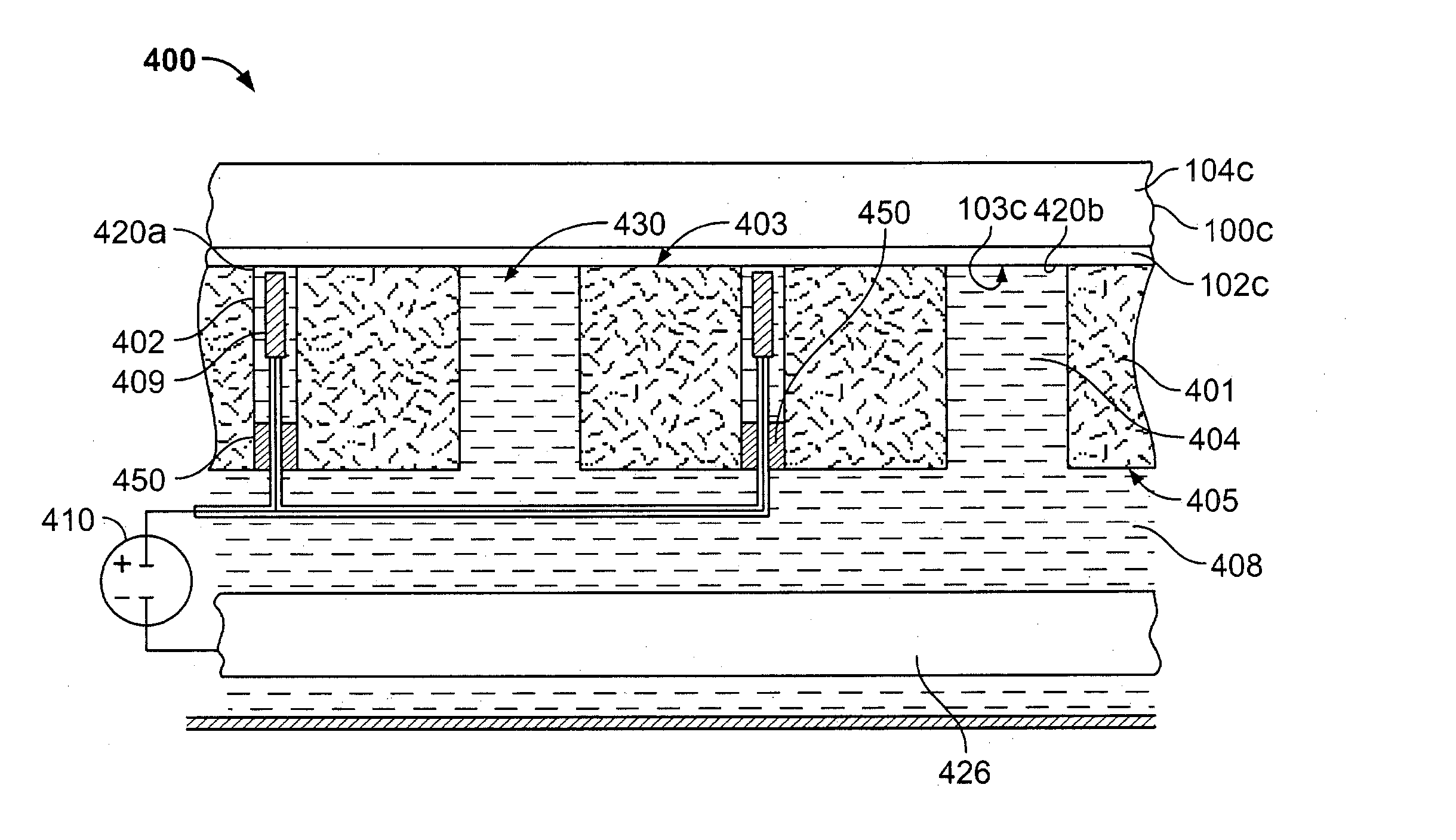
[0056] As will be described below, the present invention provides a method and a system to electroetch or electropolish a conductive material layer deposited on a surface of a semiconductor. The invention can be used with Electrochemical Mechanical Etching processes or conventional electroetching systems. The present invention achieves electroetching of the conductive material through the combination of the use of a process solution and electrical contact elements that do not make physical contact to the workpiece surface.

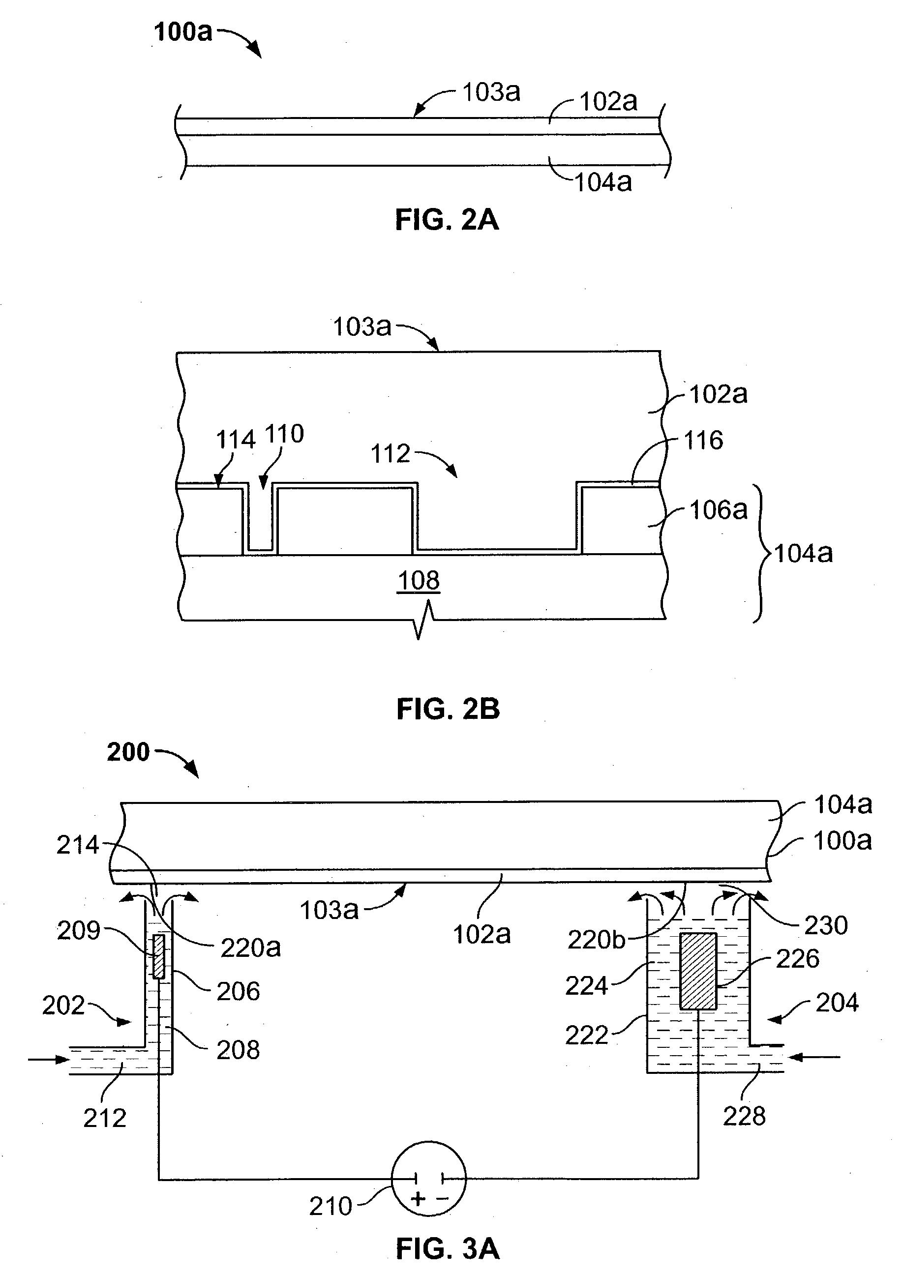
[0057] Reference will now be made to the drawings wherein like numerals refer to like parts throughout. FIG. 2A shows a cross-sectional view of a portion of a workpiece 100a. The workpiece may be an exemplary portion of a preprocessed semiconductor wafer. As also shown in FIG. 2B in detail, a top layer 102a of the workpiece 100a may include a layer of conductive material such as electroplated copper. A bottom layer 104a of the workpiece may include an insulating l...


PUM

PropertyMeasurementUnit
Flow rateaaaaaaaaaa
Electrical conductoraaaaaaaaaa
Abrasiveaaaaaaaaaa

Abstract

An apparatus for electropolishing a conductive layer on a wafer using a solution is disclosed. The apparatus comprises an electrode assembly immersed in the solution configured proximate to the conductive layer having a longitudinal dimension extending to at least a periphery of the wafer, the electrode assembly including an elongated contact electrode configured to receive a potential difference, an isolator adjacent the elongated contact electrode, and an elongated process electrode adjacent the isolator configured to receive the potential difference, a voltage supply is configured to supply the potential difference between the contact electrode and the process electrode to electropolish the conductive layer on the wafer.

Description

RELATED APPLICATIONS [0001] This application is a continuation-in-part of U.S. patent application Ser. No. 10 / 391,924 (NT-291) filed Mar. 18, 2003 and claims priority from Provisional Application Ser. No. 60 / 425,694 (NT-281P) filed Nov. 12, 2002, all incorporated herein by reference. [0002] This application is a continuation-in-part of U.S. application Ser. No. 10 / 093,185, filed Mar. 5, 2002, (NT-003C) which is a continuation of U.S. Ser. No. 09 / 877,335 filed Jun. 7, 2001 (NT-003D), now U.S. Pat. No. 6,471,847, which is a divisional of U.S. Ser. No. 09 / 283,024 filed Mar. 30, 1999 (NT-003), now U.S. Pat. No. 6,251,235, all incorporated herein by reference. [0003] This application is also a continuation-in-part of U.S. application Ser. No. 10 / 459,321 (NT-105C4) filed Jun. 10, 2003 which is a continuation of U.S. Ser. No. 09 / 685,934 filed Oct. 11, 2000 (NT-105), now U.S. Pat. No. 6,497,800 claiming priority to U.S. Prov. No. 60 / 190,023, filed Mar. 17, 2000, all incorporated herein by r...

Claims


Application Information

Patent Timeline
IPC IPC(8): B24B37/04C25D5/02C25D5/06C25D5/22C25D7/12C25F7/00H01L21/00H01L21/288H01L21/321
CPCC25F7/00H01L21/2885H01L21/32115B24B37/20H01L21/67075H01L21/6715B24B37/046H01L21/32125
Inventor BASOL, BULENT M.ASHJAEE, JALALGOVZMAN, BORISTALIEH, HOMAYOUNFREY, BERNARD M.
Owner NOVELLUS SYSTEMS
Why Eureka
Try Eureka