Methods of bridging lateral nanowires and device using same

a technology of lateral nanowires and nanowires, which is applied in the direction of nanoinformatics, instruments, polycrystalline material growth, etc., can solve the problems of difficult to provide nanowires and limited practicability of nanowires

Inactive Publication Date: 2005-06-23
HEWLETT PACKARD DEV CO LP
View PDF7 Cites 177 Cited by
  • Summary
  • Abstract
  • Description
  • Claims
  • Application Information

AI Technical Summary

Problems solved by technology

While holding much promise, the practical application of nanowires has been somewhat limited.
In particular, it has proved difficult to provide nanowires, especially laterally grown nanowi...

Method used


Image

  • Methods of bridging lateral nanowires and device using same
  • Methods of bridging lateral nanowires and device using same
  • Methods of bridging lateral nanowires and device using same

Examples


examples

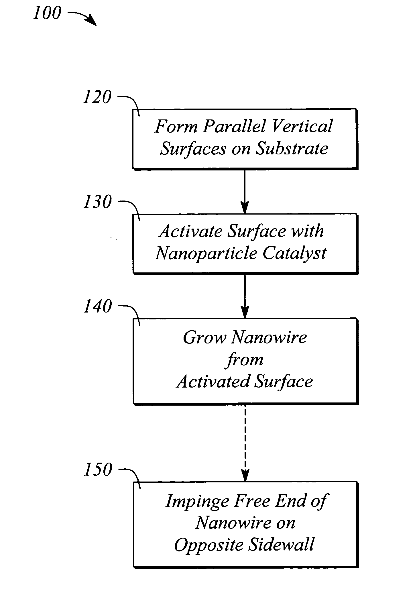
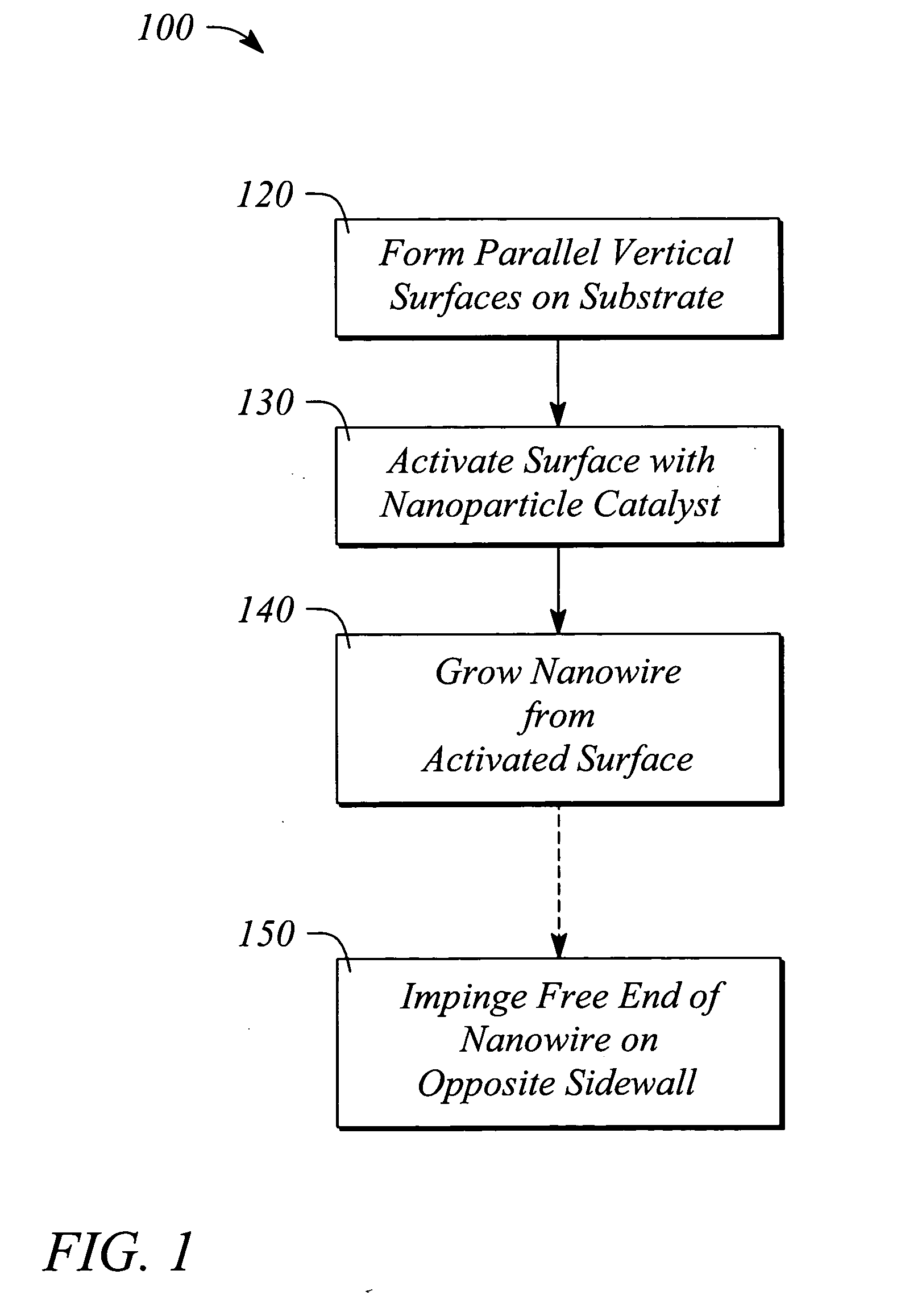
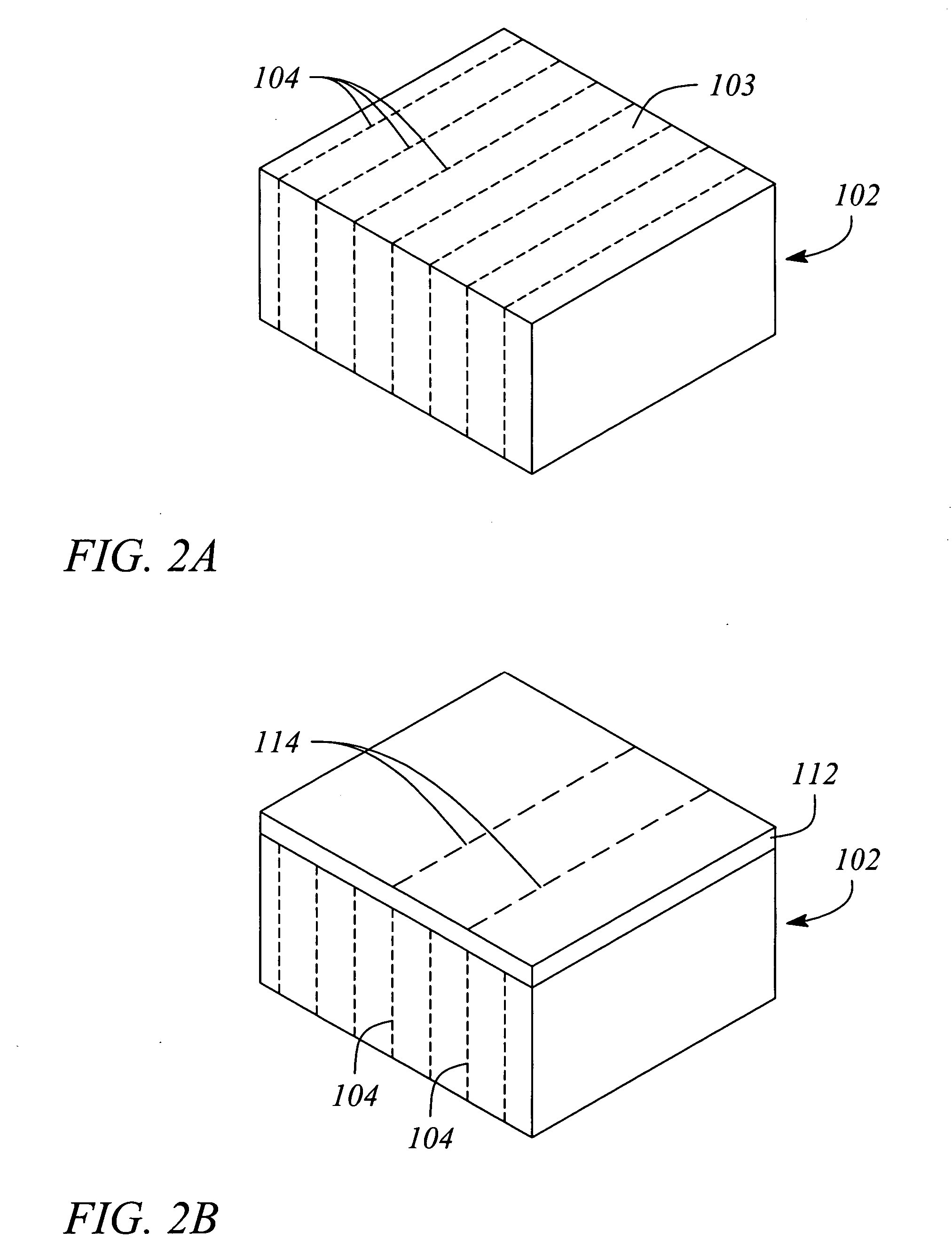
[0123] In a particular example of laterally growing nanowires as described hereinabove in various embodiments, the oxide layer is a thermal oxide that is patterned using photoresist and optical lithography to define locations of several trenches in a top surface of an (110) oriented Si substrate. Opposing sidewalls of the trenches, so defined and located, coincide with opposing pairs of (111) planes in the Si substrate.

[0124] The patterned thermal oxide layer of the substrate is then etched using reactive ion etching (RIE). For the example, RIE uses a combination of a trifluoromethane (CHF3) gas and an Argon (Ar) gas. RIE exposes portions of the silicon surface of the substrates. The exposed portions are where the trenches are to be formed. As such, the patterned etched thermal oxide layer forms an oxide mask for use in subsequent silicon etching.

[0125] Following RIE and removal of the resist layer, the substrates are etched using a liquid-phase etching solution. The etching solut...


PUM

PropertyMeasurementUnit
Angleaaaaaaaaaa
Angleaaaaaaaaaa
Angleaaaaaaaaaa

Abstract

A semiconductor nanowire is grown laterally. A method of growing the nanowire forms a vertical surface on a substrate, and activates the vertical surface with a nanoparticle catalyst. A method of laterally bridging the nanowire grows the nanowire from the activated vertical surface to connect to an opposite vertical surface on the substrate. A method of connecting electrodes of a semiconductor device grows the nanowire from an activated device electrode to an opposing device electrode. A method of bridging semiconductor nanowires grows nanowires between an electrode pair in opposing lateral directions. A method of self-assembling the nanowire bridges the nanowire between an activated electrode pair. A method of controlling nanowire growth forms a surface irregularity in the vertical surface. An electronic device includes a laterally grown nano-scale interconnection.

Description

STATEMENT REGARDING FEDERALLY SPONSORED RESEARCH OR DEVELOPMENT [0001] The U.S. Government has a paid-up license in this invention and the right in limited circumstances to require the patent owner to license others on reasonable terms as provided for by the terms of Contract No. MDA972-01-3-0005 awarded by the Defense Advanced Research Projects Agency.BACKGROUND [0002] 1. Technical Field [0003] The invention relates to nano-scale semiconductor devices and fabrication methods therefor. In particular, the invention relates to fabrication and use of nanowires in semiconductor devices. [0004] 2. Description of Related Art [0005] A consistent trend in semiconductor technology since its inception is toward smaller and smaller device dimensions and higher and higher device densities. As a result, an area of semiconductor technology that recently has seen explosive growth and generated considerable interest is nanotechnology. Nanotechnology is concerned with the fabrication and application...

Claims


Application Information

Patent Timeline
IPC IPC(8): D01F9/127H01L21/768H01L23/532H01L51/30
CPCB82Y10/00B82Y30/00G11C13/025G11C2213/16G11C2213/17H01L21/76838H01L23/53271H01L2924/0002H01L2221/1094Y10S977/742Y10S977/721H01L2924/00
Inventor ISLAM, M. SAIFKAMINS, THEODORE I.SHARMA, SHASHANK
Owner HEWLETT PACKARD DEV CO LP
Why Eureka
Try Eureka