Electron beam system and method of manufacturing devices using the system

a technology of electron beam and manufacturing device, applied in the field of electron beam system, can solve the problems of difficult evaluation of samples with high throughput, poor s/n ratio, large shot noise of electron beam, etc., and achieve the effects of small shot noise, lower throughput, and higher beam curren

Inactive Publication Date: 2005-06-23
EBARA CORP
View PDF12 Cites 20 Cited by
  • Summary
  • Abstract
  • Description
  • Claims
  • Application Information

AI Technical Summary

Benefits of technology

[0012] One of the subjects to be accomplished by the invention is to provide an electron beam system that can provide an evaluation of a sample with high throughput by reducing a shot noise of an electron beam and thereby improving the S / N ratio.
[0013] Another subject to be accomplished by the present invention is to provide an electron beam system that allows a beam current to be made higher and thus can evaluate a sample with high throughput.
[0014] Still another subject to be accomplished by the present invention is to provide a fully furnished system for a defect inspection apparatus by manufacturing an electron optical column employing only two stage of lenses to form and control a shaped beam with high stability.
[0017] The present invention has been made to solve the problems pointed out above, and the object thereof is to provide an electron beam system which comprises an axisymmetric filter as well as an electron gun with a smaller shot noise, and allows a relatively higher beam current to be obtained as compared to that which can be achieved by using an electron gun with the same brightness, and also to provide a defect inspection method using the same electron beam system, as well as a device manufacturing method using the same electron beam system and defect inspection method.
[0018] There has been a problem that if both rough alignment and fine alignment are carried out, it takes a long time to complete an alignment operation, resulting in a lower throughput (a quantity of processing per unit time) achieved by the inspection apparatus. In addition, when an electron optical system is used to conduct alignment, an electron beam dose equivalent to or greater than that applied in the sample evaluation would be applied to the wafer, which in turn could destroy a gate oxide or the like. The present invention is also directed to solving the above problem. Accordingly, another object of the present invention is to provide an inspection apparatus, in which inspection of a wafer can be carried out by conducting alignment without using any electron beams, and thus without destroying the gate oxide and the like. Another object of the present invention is to provide a device manufacturing method using such an inspection apparatus as described above.
[0030] An inspection apparatus for evaluating a fine geometry on a surface of a sample according to the present invention comprises: an electron optical system including a primary optical system for irradiating an electron beam against a sample and a detecting system for detecting the electron beam emanated from the sample; a movable stage for carrying the sample and moving the sample relative to the electron optical system; and a position sensor capable of measuring a position of the sample with a desired precision. The position sensor is disposed in a location spaced by a desired distance from the electron optical system, and the movable stage is moved on the basis of a position signal output from the position sensor so as to bring the sample into a reference position in said electron optical system with a desired precision. The inspection apparatus, in the condition where the sample has been matched to the reference position in the electron optical system with the desired precision, acquires an SEM image of a surface of the sample by the electron optical system and the thus acquired SEM image is compared to another acquired SEM image or to a reference image for the pattern matching, thereby allowing for competitive evaluation.

Problems solved by technology

However, it is problematic that although in a schottky electron gun, a beam current three to ten times higher as compared to that obtained by a thermionic emission electron gun (e.g., LaB6 electron gun) can be obtained, and a shot noise of the electron beam is quite large and inevitably an S / N ratio is not so good, which makes it difficult to evaluate a sample with high throughput.
On the other hand, the crossover image demagnification type beam by using the LaB6 electron gun also has a drawback such that it is impossible to make the beam current higher, and this makes it difficult to evaluate a sample with high throughput.
It is also problematic that the space charge effect becomes greater in proportion to the length of the optical path, and it is difficult to accomplish a good intensity and position stability of the electron beam.

Method used


Image

  • Electron beam system and method of manufacturing devices using the system
  • Electron beam system and method of manufacturing devices using the system
  • Electron beam system and method of manufacturing devices using the system

Examples


first embodiment

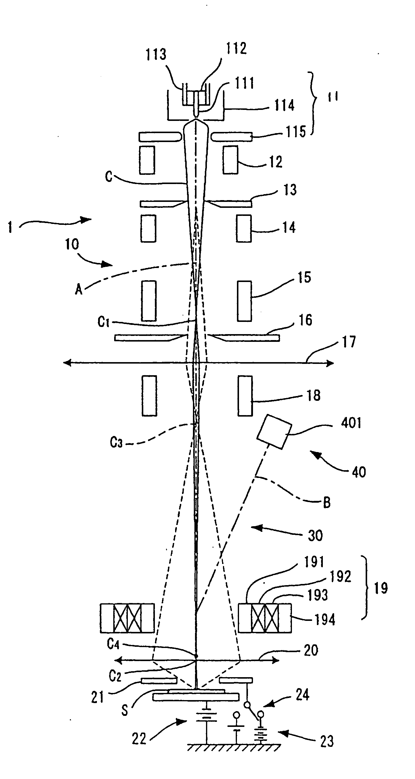
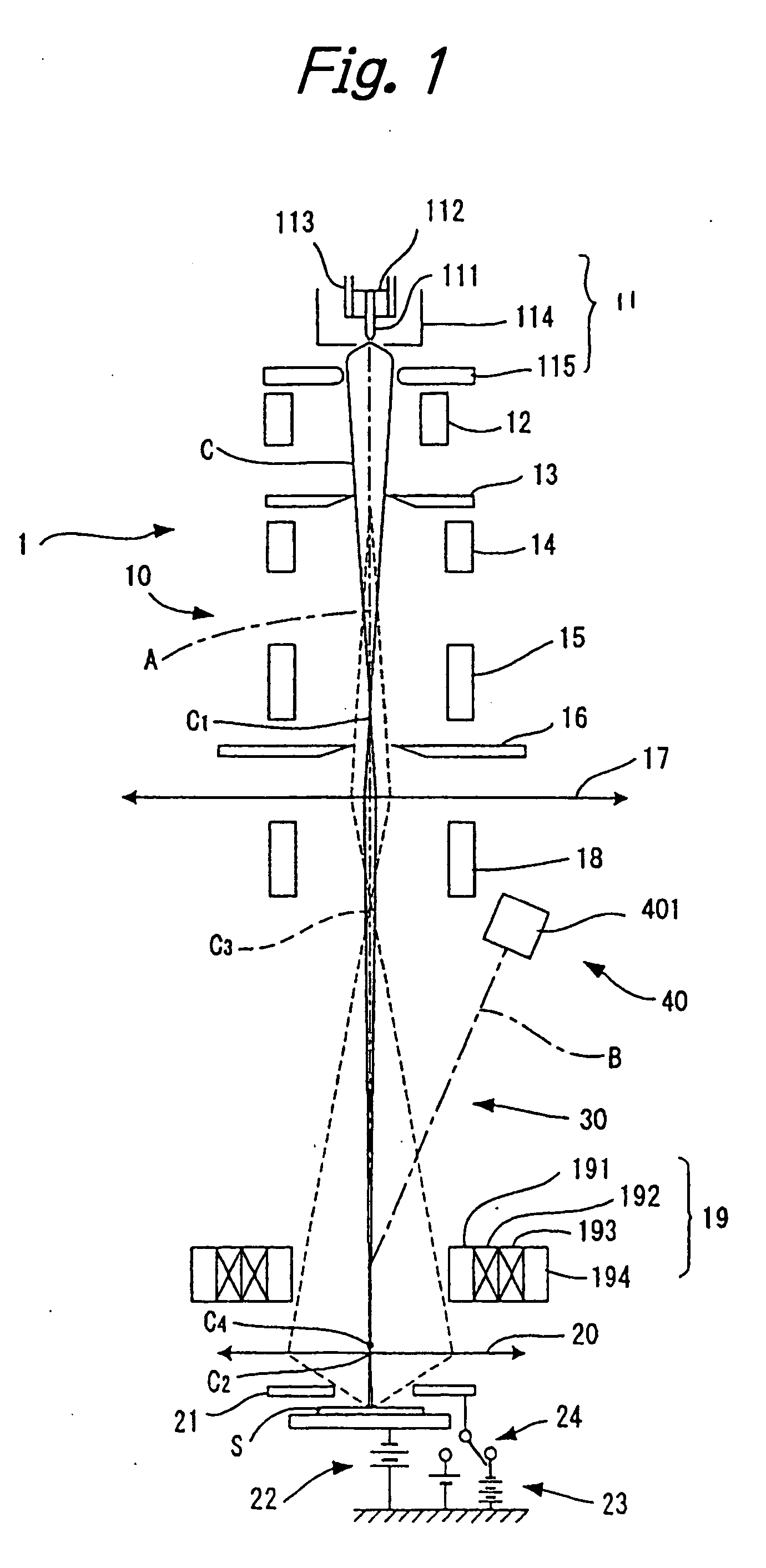
[0051] In the first embodiment, the electron gun 11 is implemented as a LaB6 electron gun of the thermionic emission type, which comprises a LaB6 cathode 111, a graphite heater 112, a support fittings 113, a Wehnelt electrode 114 and an anode 115. By adjusting a bias of the Wehnelt electrode 114 of the electron gun 11 to be deeper to some extent, the electron gun 11 can be controlled within a space charge limited condition. The shaping aperture 13 is square in shape and disposed in a location in the electron gun side with respect to the NA aperture 16. Further, both of the two-stage lenses (i.e., the condenser lens 17 and the objective lens 20) are disposed in front locations of the shaping aperture 13 and the NA aperture 16 (i.e., in the sample side which is in a forward side with respect to the direction along which the electron beam advances).

[0052] The secondary optical system 30 is serving as an optical system for introducing secondary electrons emanated from the sample S into ...

second embodiment

[0062] An operation of the electron beam system having the configuration designated above will now be described. An electron beam “C” emitted from the electron gun 11 passes through the shaping aperture 13 to form a crossover image “C1′” in a predetermined location between the shaping aperture 13 and the condenser lens 17, and then the beam is dispersed from the crossover image C1′ at a spreading angle that is not too great. The dispersed electron beam is converged by the condenser lens 17 to form a crossover image “C2′” in the NA aperture 16. After forming the crossover image C2′, the electron beam proceeds toward the sample S and is directed to the sample S by the objective lens 20. An image of the shaping aperture 13 is demagnified by the condenser lens 17 and the objective lens 20 into the image on the sample S. In order to scan the sample, the beam is deflected in a two-stage manner by using the electrostatic deflector 18 and the electrostatic deflector 25 for scanning.

[0063] ...

third embodiment

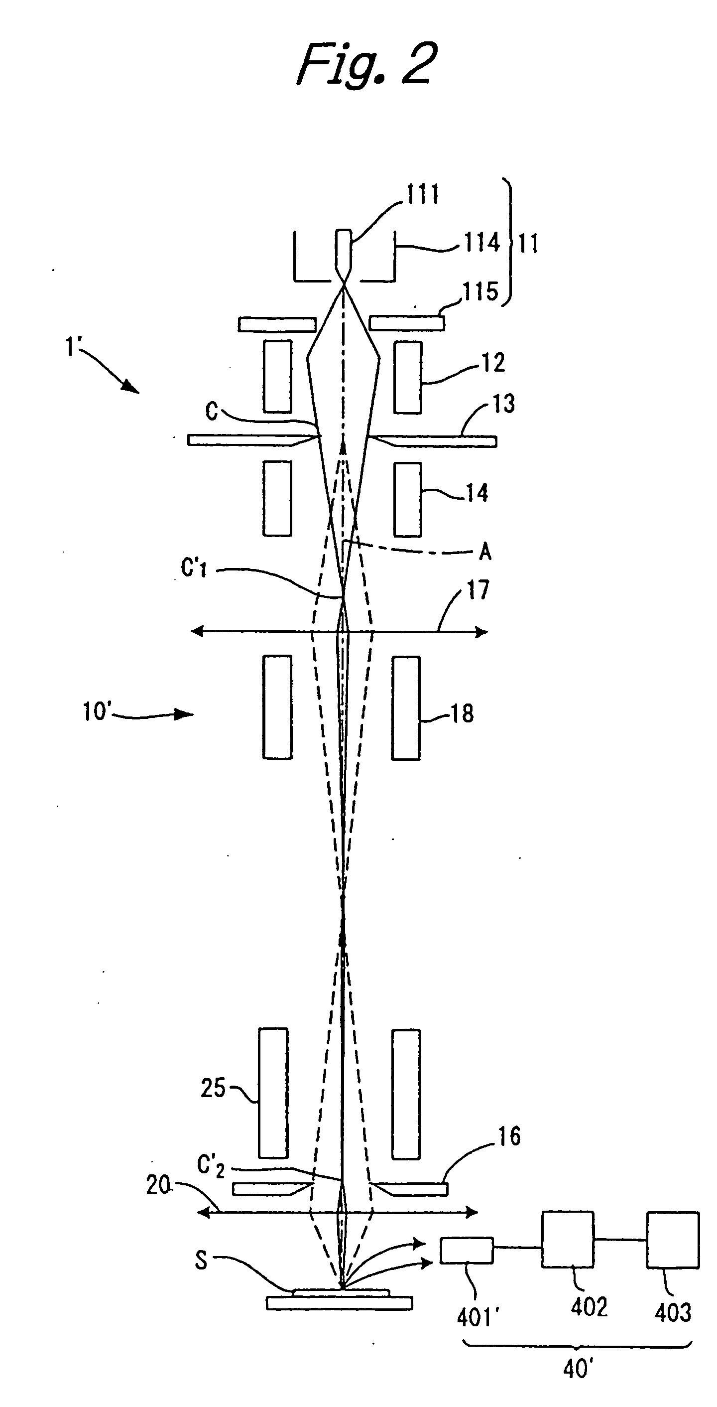
[0065] Some further embodiments of the present invention will now be described below with reference to FIG. 3 to FIG. 6. FIG. 3 shows one example of configuration of an electron optical system in an electron beam system according to the present invention. In FIG. 3, an electron gun 11 comprises a cathode 201 made of LaB6 single crystal, a Wehnelt 202 and an anode 203, which are operated within a space charge limited condition. A primary electron beam emitted from the electron gun 11 is converged by a first condenser lens 204 to form a crossover image in a second aperture plate 205. A first aperture plate 206 has a square opening and thereby enables a high beam current (an intensified primary electron beam) to be obtained. It is to be noted that if a slightly deteriorated resolution in any specific direction is permissible, then a rectangular opening, instead of the square opening, may be used. The first aperture plate 206 having a shaping aperture is disposed downstream to the first...


PUM

PropertyMeasurementUnit
widthaaaaaaaaaa
widthaaaaaaaaaa
thicknessaaaaaaaaaa

Abstract

An electron beam system wherein a shot noise of an electron beam can be reduced and a beam current can be made higher, and further a shaped beam is formed by a two-stage lenses so as to allow for an operation with high stability. In this electron beam system, an electron beam emitted from an electron gun is irradiated onto a sample and secondary electrons emanated from the sample are detected. The electron gun is a thermionic emission type and designed to operate in a space charge limited condition. A shaping aperture and a NA aperture are arranged in front locations of the electron gun. An image of the shaping aperture formed by an electron beam emitted from the thermionic emission electron gun is focused onto a surface of the sample through the two-stage lenses.

Description

BACKGROUND OF THE INVENTION [0001] The present invention relates to an electron beam system, a defect inspection apparatus for a device, which employs the same electron beam system, and a manufacturing method of a device using the same defect inspection apparatus, and more specifically, relates to an electron beam system which can evaluate a sample (a semiconductor wafer) having a device pattern with a minimum line width equal to or less than 0.1 μm with both a high throughput and high reliability, a defect inspection apparatus for a device, which employs the same electron beam system, and a manufacturing method of a device which can improve a yield thereof by evaluating a wafer after it has been processed using the same defect inspection apparatus. [0002] The present invention also relates to an electron beam system and a defect inspection method for evaluating a device, such as a wafer or a mask, having a pattern with a minimum line width in a range of 0.1 micron, and also to a me...

Claims


Application Information

Patent Timeline
Patent Type & Authority Applications(United States)
IPC IPC(8): G01N23/04G21K7/00H01J37/28
CPCG01N23/04H01J2237/2817H01J37/28G01N23/2251
Inventor NAKASUJI, MAMORUKATO, TAKAOSATAKE, TOHRUWATANABE, KENJIMURAKAMI, TAKESHINOJI, NOBUHARU
Owner EBARA CORP
Why Eureka
Try Eureka