Integrated circuit package substrate having a thin film capacitor structure

a technology of integrated circuit package and capacitor structure, which is applied in the direction of printed capacitor incorporation, printed circuit aspects, printed capacitor incorporation, etc., can solve the problems of large amount of real estate occupied by the substrate, difficult to drill holes therein, and brittle silicon

Inactive Publication Date: 2005-06-23
INTEL CORP
View PDF2 Cites 24 Cited by
  • Summary
  • Abstract
  • Description
  • Claims
  • Application Information

AI Technical Summary

Problems solved by technology

Discrete capacitors are relatively large and thus take up a large amount of real estate on a substrate.
Silicon is a brittle material, which makes it difficult to drill openings therein.

Method used


Image

  • Integrated circuit package substrate having a thin film capacitor structure
  • Integrated circuit package substrate having a thin film capacitor structure
  • Integrated circuit package substrate having a thin film capacitor structure

Examples


Embodiment Construction

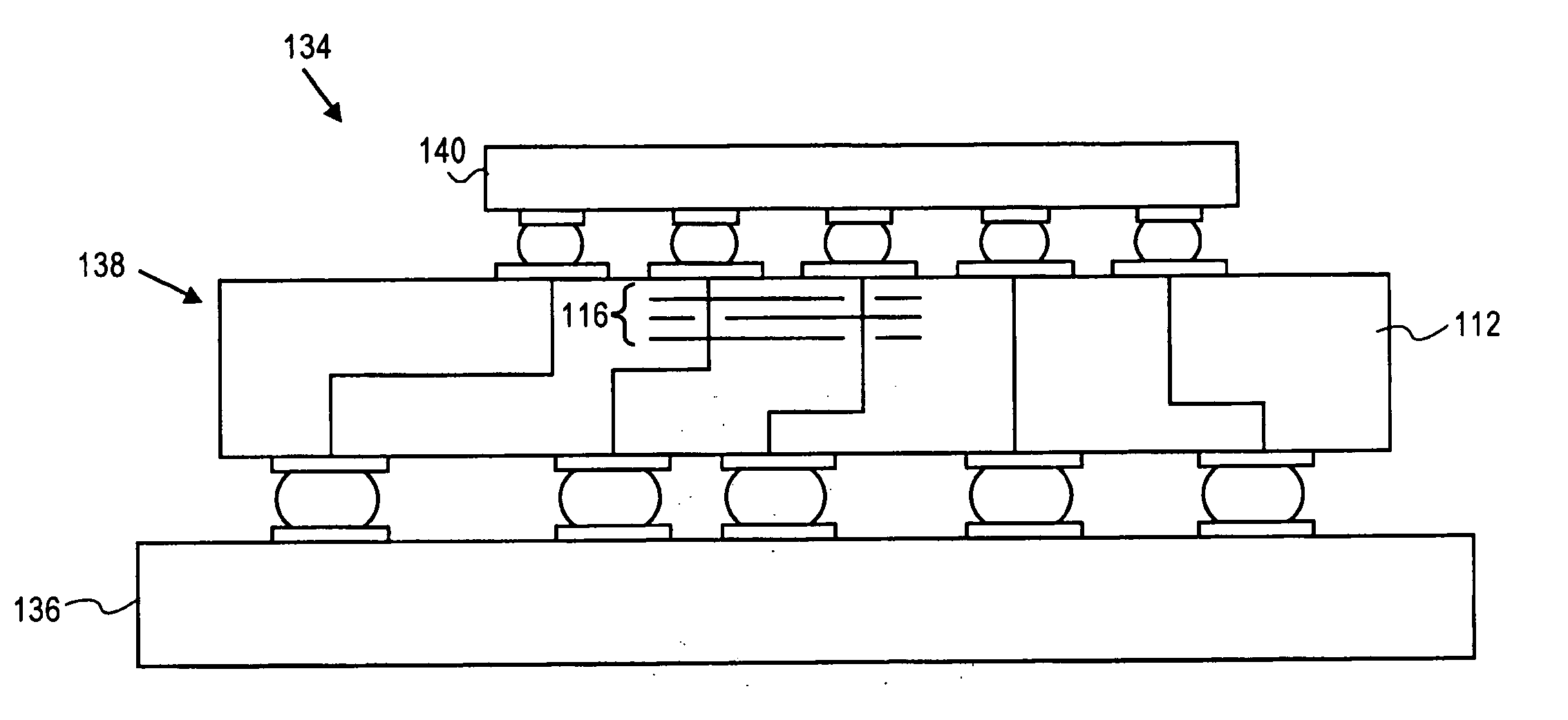
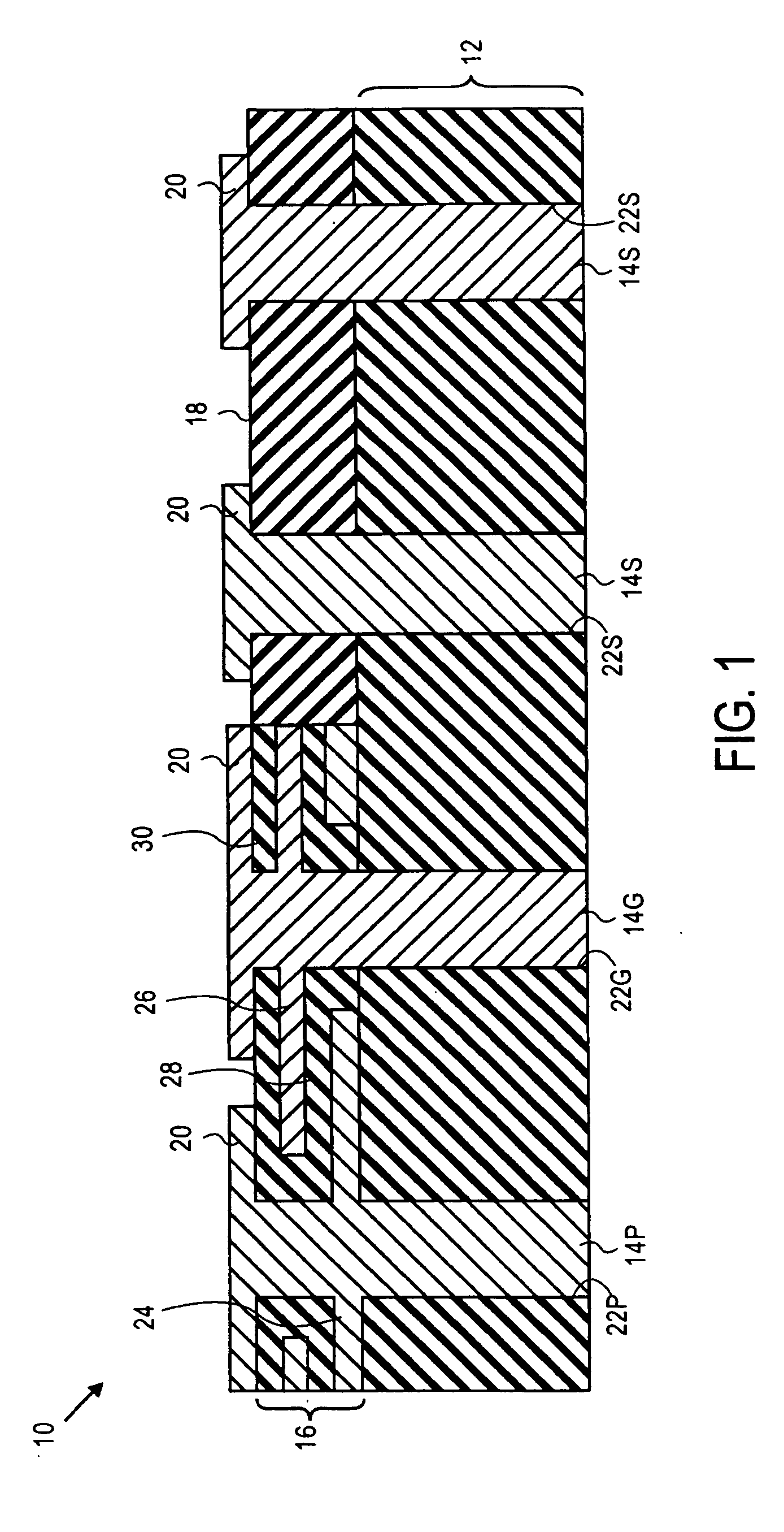
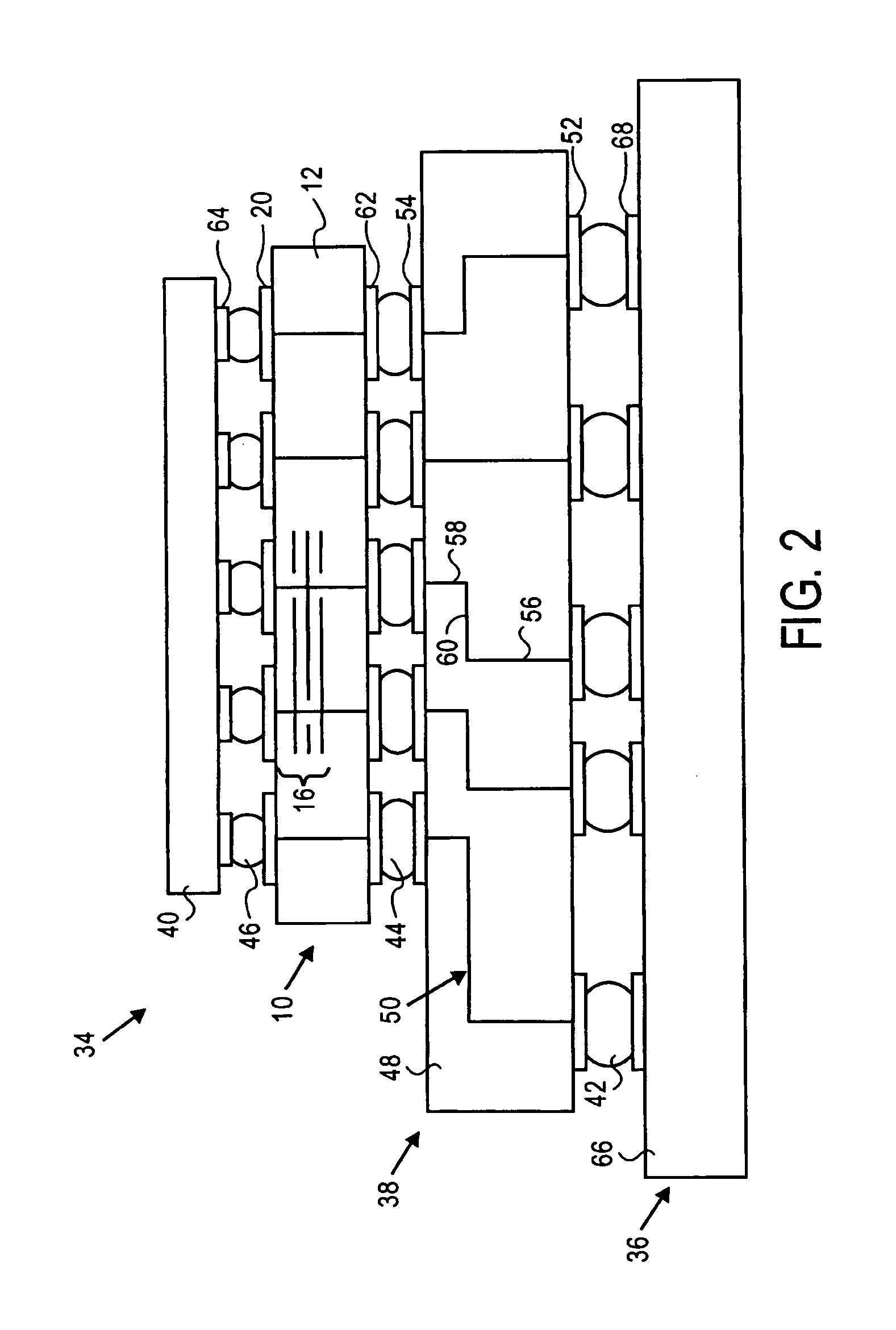
[0013] The manufacture of a substrate, such as a package substrate or an interposer substrate, of an integrated circuit package is described. A base structure is formed from a green material having a plurality of via openings therein. The green material is then sintered so that the green material becomes a sintered ceramic material and the base structure becomes a sintered ceramic base structure having the via openings. A conductive via is formed in each via opening of the sintered ceramic base structure. A capacitor structure is formed on the sintered ceramic base structure. The power and ground planes of the capacitor structure are connected to the vias. As such, a capacitor structure can be formed and connected to the vias without the need to drill via openings in brittle substrates such as silicon substrates. The sintered ceramic material also has a low coefficient of thermal expansion and can resist high temperature processing conditions when manufacturing the capacitor structu...


PUM

PropertyMeasurementUnit
dielectric constantaaaaaaaaaa

Abstract

This invention relates to the manufacture of a substrate, such as a package substrate or an interposer substrate, of an integrated circuit package. A base structure is formed from a green material having a plurality of via openings therein. The green material is then sintered so that the green material becomes a sintered ceramic material and the base structure becomes a sintered ceramic base structure having the via openings. A conductive via is formed in each via opening of the sintered ceramic base structure. A capacitor structure is formed on the sintered ceramic base structure. The power and ground planes of the capacitor structure are connected to the vias. As such, a capacitor structure can be formed and connected to the vias without the need to drill vias openings in brittle substrates such as silicon substrates. The sintered ceramic material also has a low coefficient of thermal expansion and can resist high temperature processing conditions when manufacturing the capacitor structure, and is inexpensive to manufacture.

Description

BACKGROUND OF THE INVENTION [0001] 1). Field of the Invention [0002] This invention relates to a capacitor structure that is included in a substrate of an integrated circuit package. [0003] 2). Discussion of Related Art [0004] Integrated circuits are usually manufactured on wafer substrates. Wafer substrate is then “diced” or “singulated” into individual dies, each die carrying a respective integrated circuit. The die is then mounted on a package substrate, often with an intermediate interposer substrate. The substrate or substrates provide structural rigidity to the resulting integrated circuit package. A package substrate also provides x-y transformation from contacts of the die to contacts on a carrier substrate on which the integrated circuit package is mounted. [0005] Signals can be provided through conductors in the substrate or substrates to and from an integrated circuit in the die. Signal delay, referred to as resistance-capacitance-inductance delay, often occurs when signa...

Claims


Application Information

Patent Timeline
Patent Type & Authority Applications(United States)
IPC IPC(8): H01L23/498H01L23/64H05K1/03H05K1/16
CPCH01L23/49822H01L23/642H01L2224/16H01L2924/01078H01L2924/15174H01L2924/01019H05K1/0306H05K1/162H05K3/4688H05K2201/0187H05K2201/09309H01L2924/15311H01L2224/05568H01L2224/05573H01L2924/00014H01L2224/05599
Inventor PALANDUZ, CENGIZ A.
Owner INTEL CORP
Why Eureka
Try Eureka