Packaging substrates for integrated circuits and soldering methods

a technology of integrated circuits and substrates, which is applied in the direction of electrical equipment, semiconductor devices, semiconductor/solid-state device details, etc., can solve the problems of shortening the electrical connection, reducing the package size, and reducing the soldering efficiency of flip-chip packaging, so as to reduce the manufacturing process, simplify the solder hierarchy, and increase the melting temperature

Active Publication Date: 2005-06-23
INVENSAS CORP
View PDF17 Cites 93 Cited by
  • Summary
  • Abstract
  • Description
  • Claims
  • Application Information

AI Technical Summary

Benefits of technology

[0016] Soldering: In some embodiments of the present invention, maintaining the solder hierarchy is simplified through changing the solder melting temperature during soldering. It is well known that a solder melting temperature may increase if a soldered surface contains copper because the copper may dissolve in the solder during the soldering operation to raise the solder melting temperature. In some embodiments, this property is used to obtain a proper solder hierarchy. For example, in some embodiments, all of the sequential soldering operations use the same starting solder material. In each soldering operation, the solder's melting temperature increases, so the solder will not melt in the subsequent soldering operations. The manufacturing process is simplified because it eliminates the need to obtain different solder types with different initial melting temperatures.

Problems solved by technology

The flip chip packaging reduces the package size and shortens the electrical connections between the die and the PCB, but the flip chip packaging is vulnerable to solder failures caused by thermal expansion and contraction.
The solder failures are due to the differences in the coefficient of thermal expansion (CTE) between the die and the PCB.
However, thin interposers are fragile, can be warped, and their heat dissipation capabilities are poor, so the interposer handling is complicated.
However, in a packaging substrate, the interposer may have to be thinned to its final thickness before the die attachment.

Method used


Image

  • Packaging substrates for integrated circuits and soldering methods
  • Packaging substrates for integrated circuits and soldering methods
  • Packaging substrates for integrated circuits and soldering methods

Examples


Embodiment Construction

[0023] The embodiments described in this section illustrate but do not limit the invention. The invention is not limited to particular materials, process steps, or dimensions. The invention is defined by the appended claims.

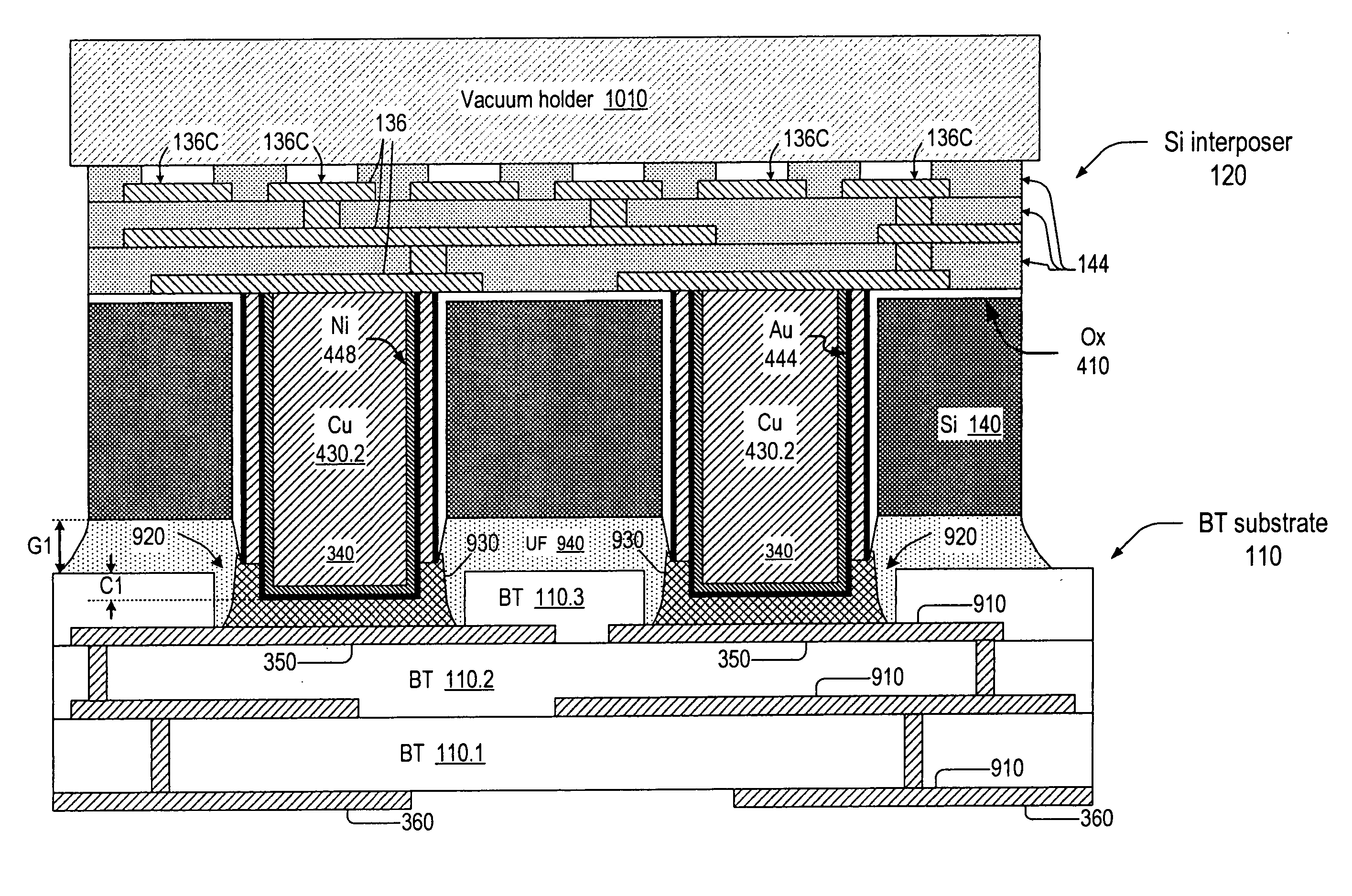
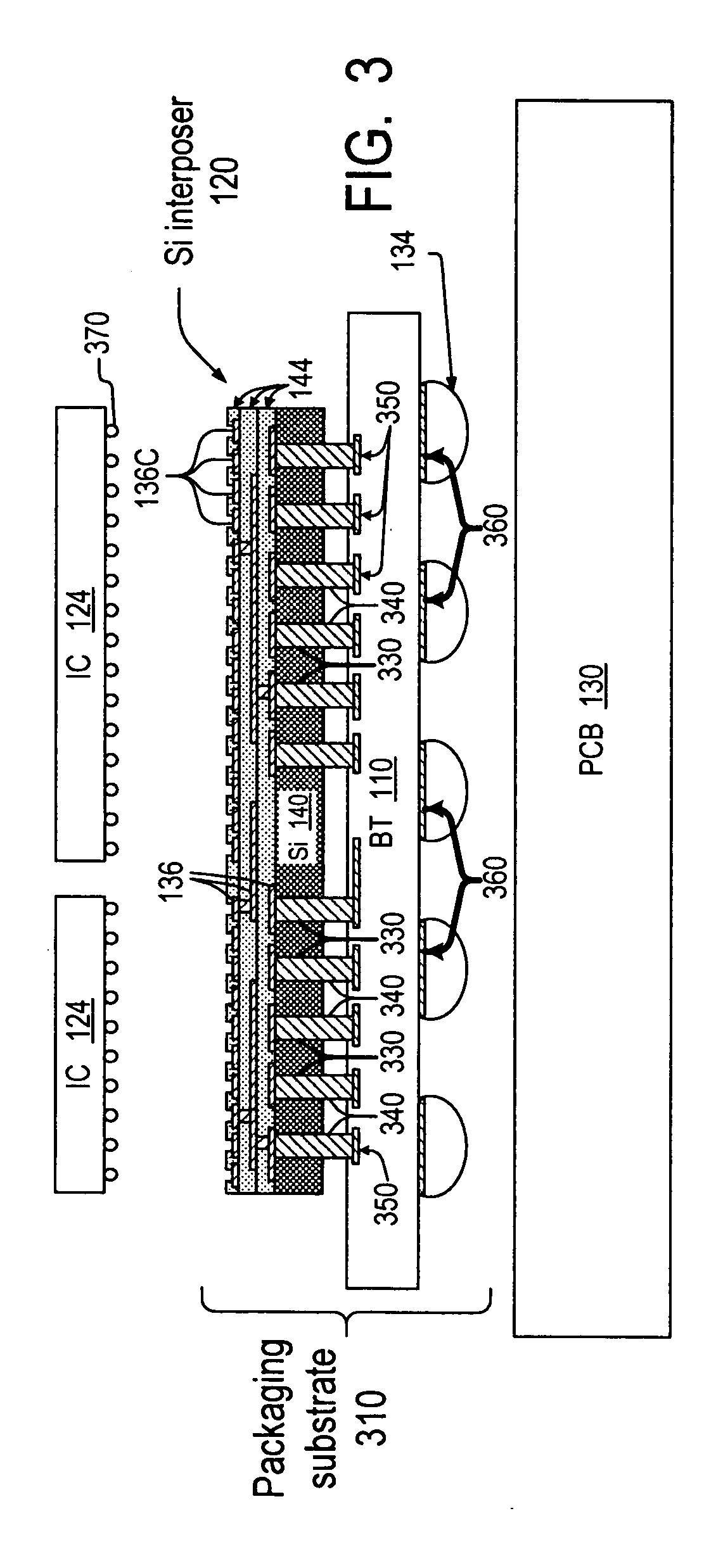
[0024]FIG. 3 illustrates an integrated circuit packaging substrate 310 having two intermediate integrated circuit packaging substrates 110, 120. Substrate 120 is a silicon interposer attached to BT substrate 110. Dies 124 and PCB 130 will be attached later.

[0025] Silicon interposer 120 includes metal layers 136 formed over silicon substrate 140. Substrate 140 has substantially planar top and bottom surfaces, and is quite thin. In some embodiments, the planarity of substrate 140 is suitable for fine geometry photolithography (finer than possible with BT and FR4 substrates). The thickness of substrate 140 can be 100 μm or less (50 μm to 35 μm thickness values believed to be achievable, and smaller values may be possible). Layers 136 provide interconnect lines and...


PUM


Abstract

A packaging substrate (310) includes a semiconductor interposer (120) and at least one other intermediate substrate (110), e.g. a BT substrate. The semiconductor interposer has first contact pads (136C) attachable to dies (124) above the interposer, and second contact pads (340) attachable to circuitry below the interposer. Through vias (330) are made in the semiconductor substrate (140) of the interposer (120). Conductive paths going through the through vias connect the first contact pads (136C) to the second contact pads (340). The dies (124) are attached to the interposer after the attachment of the interposer to the BT substrate. In sequential soldering operations, the solder hierarchy is maintained by dissolving some material (e.g. copper) in the solder during soldering to raise the solder's melting temperature. For example, all of the solders may initially have the same melting temperature, but each solder's melting temperature is increased during soldering to prevent the solder from melting in the subsequent soldering operations.

Description

BACKGROUND OF THE INVENTION [0001] The present invention relates to packaging of integrated circuits and to soldering methods. [0002] Integrated circuit dies (“chips”) can be attached to a lead frame and then packaged in a ceramic or plastic carrier. The leads of the lead frame can then be soldered to a printed circuit board (PCB). Alternatively, the chip can be soldered directly to the PCB (“flip chip” packaging). The flip chip packaging reduces the package size and shortens the electrical connections between the die and the PCB, but the flip chip packaging is vulnerable to solder failures caused by thermal expansion and contraction. The solder failures are due to the differences in the coefficient of thermal expansion (CTE) between the die and the PCB. [0003] The CTE mismatch has been addressed by providing an intermediate substrate between the die and the PCB, with an intermediate CTE. For example, in a ball grid array (BGA) package, the die is flip-chip attached to the intermedi...

Claims


Application Information

Patent Timeline
Patent Type & Authority Applications(United States)
IPC IPC(8): H01L21/60H01L21/768H01L23/14H01L23/48H01L23/498H01L23/538H01L25/065H05K3/34
CPCH01L23/147H01L2224/73257H01L23/49827H01L23/5384H01L23/5385H01L25/0655H01L2224/48227H01L2224/81801H01L2224/83192H01L2924/01078H01L2924/01079H01L2924/15311H01L2924/19041H01L2924/19107H01L2924/30107H01L24/48H01L2924/01322H01L2224/81191H01L2924/10253H01L23/481H01L2924/00H01L2924/14H01L2924/00014H01L2224/45099H01L2224/45015H01L2924/207
Inventor SAVASTISUK, SERGEYHALAHAN, PATRICK B.KAO, SAM
Owner INVENSAS CORP
Why Eureka
Try Eureka