Semiconductor device, RFID tag and label-like object

a technology of rfid tag and label, applied in the direction of semiconductor/solid-state device details, mechanical actuation of burglar alarms, instruments, etc., can solve the problems of large amount of facility investment, difficult to expand the use of rfid technology, and difficult to manufacture ic chips at low cost, etc., to achieve low cost, improve impact resistance, and high productivity

Active Publication Date: 2005-06-23
SEMICON ENERGY LAB CO LTD
View PDF36 Cites 113 Cited by
  • Summary
  • Abstract
  • Description
  • Claims
  • Application Information

AI Technical Summary

Benefits of technology

[0018] According to the invention, a semiconductor device capable of communicating data stored in a memory or data to be stored in a memory through a communication circuit by radio communication can be provided with high productivity at low cost by manufacturing the semiconductor device with TFTs formed over an insulating substrate. In addition, it is possible to improve impact resistance and to prevent deterioration in crystal characteristics due to distortion of a crystal structure.

Problems solved by technology

They say that it is difficult to expand the use of the RFID technology unless the RFID tag drops in price to 10 yen or less.
However, a large amount of facility investment is required to build a new production line of IC chips adopting a manufacturing technique of a semiconductor integrated circuit.
Accordingly, it becomes difficult to manufacture IC chips at low cost.
When running cost is added, it becomes very difficult to make a unit price of the IC chip 100 yen or less.
Therefore, it is very difficult to secure sufficient supply.
Thus, production of an RFID tag based on a manufacturing technique of a semiconductor integrated circuit has a problem with cost and stable supply in terms of quantity.
In addition, an IC chip manufactured by using a single crystal silicon substrate has a cleavage plane and has an essential problem that it is sensitive to impact and bending stress.
Since scraping an ultra-pure single crystal silicon substrate wastes resources and generates industrial waste, a problem is left also in terms of an environmental issue.

Method used


Image

  • Semiconductor device, RFID tag and label-like object
  • Semiconductor device, RFID tag and label-like object
  • Semiconductor device, RFID tag and label-like object

Examples


Embodiment Construction

[0038] An embodiment mode of the present invention is hereinafter described with reference to the attached drawings. Note that the present invention is not limited to the following description. As is easily known to a person skilled in the art, the mode and the detail of the invention can be variously changed without departing from the purpose and the scope of the present invention. Therefore, the present invention is not interpreted limiting to the following description of the embodiment mode. Note that the same reference numeral is given to the same portion or a portion having a similar function among different diagrams to be described hereinafter, and repetitive description is omitted.

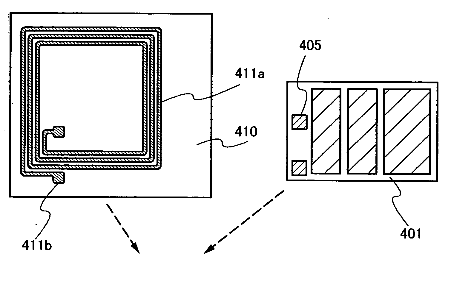
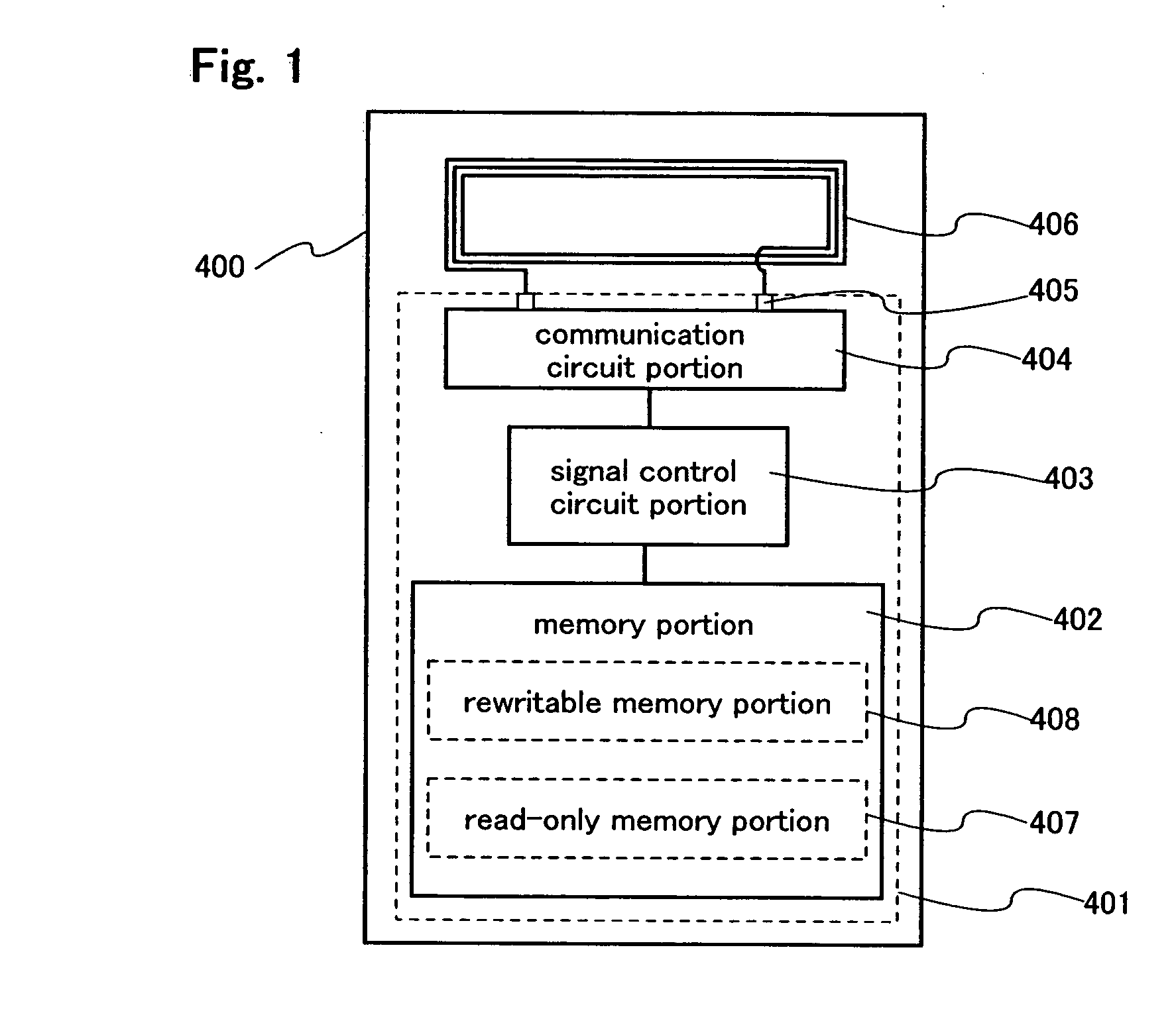
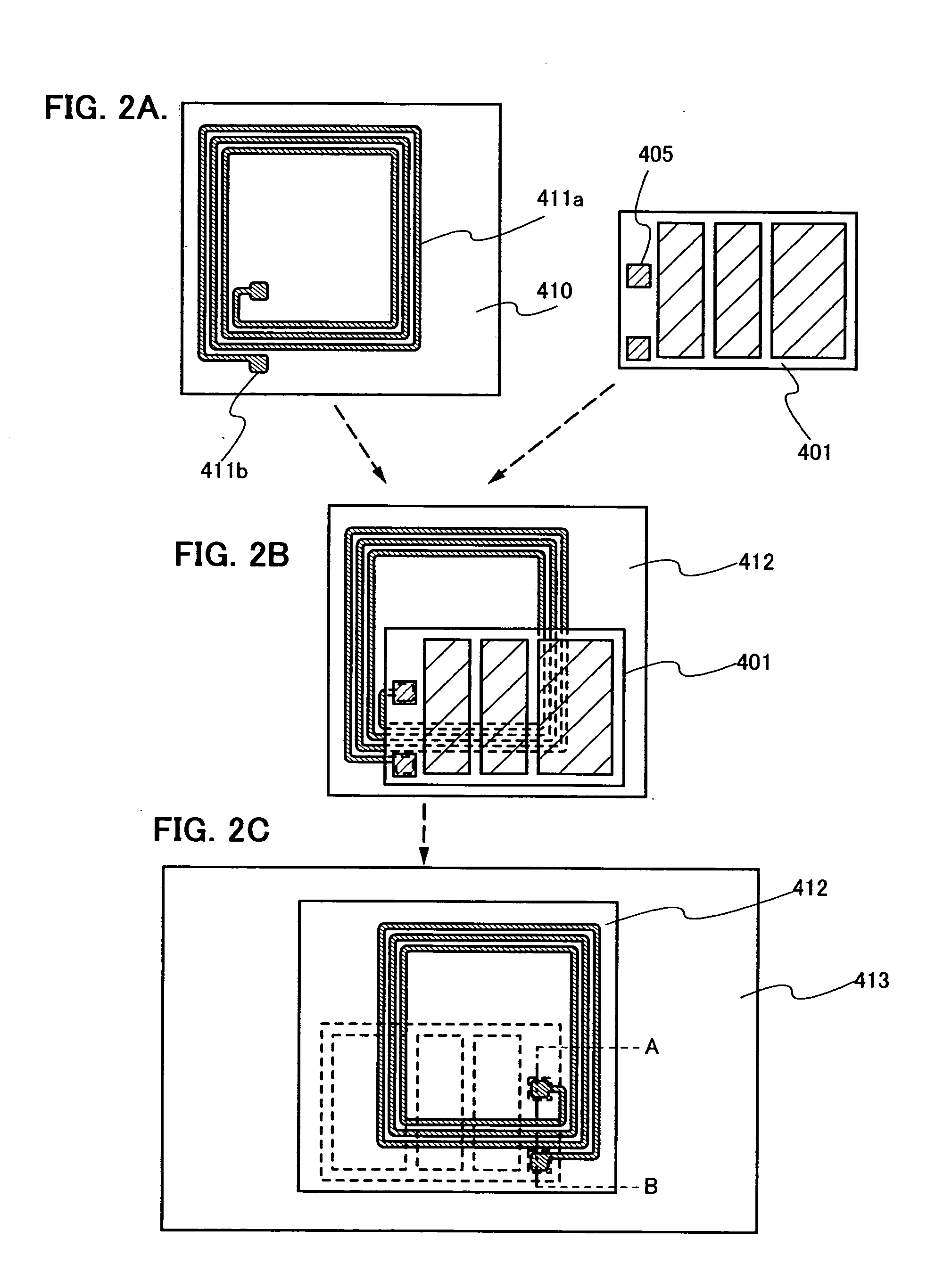
[0039]FIG. 1 is a block diagram showing a main structure of an RFID semiconductor device 400 of the present invention. In an ID chip 401, a memory portion 402, a signal control circuit portion 403 and a communication circuit portion 404 are formed with the use of a TFT formed over an insulating sub...


PUM

PropertyMeasurementUnit
areaaaaaaaaaaa
widthaaaaaaaaaa
widthaaaaaaaaaa

Abstract

An object of the present invention is to supply a semiconductor device capable of communicating data through radio communication, such as an RFID tag or a label-like object, with high productivity at low cost. In the invention, a memory portion, a signal control circuit portion and a communication circuit portion are formed with the use of a TFT formed over an insulating substrate, and the insulating substrate is fixed opposite to a support provided with an antenna so that the antenna is connected to a terminal portion connected to a communication circuit. The invention is an RFID tag and a label-like object including an ID chip whose memory portion, signal control portion and communication circuit portion are formed with the use of TFTs formed over an insulating substrate and an antenna formed to connect to a terminal portion of the ID chip, in which data stored in a memory portion or data to be stored in a memory portion can be communicated through a communication circuit by radio communication.

Description

BACKGROUND OF THE INVENTION [0001] 1. Field of the Invention [0002] The present invention relates to a semiconductor device which transmits and receives data through radio communication. Specifically, the invention relates to a semiconductor device in which an integrated circuit is formed with a thin film over an insulating substrate containing glass or the like and to an ID tag and a label-like object using the semiconductor device. [0003] 2. Description of the Related Art [0004] A technology referred to as radio frequency identification (also referred to as RFID) has been attracting attention in place of a code referred to as a barcode used for identifying products and the like. RFID is an automatic identification technique utilizing radio communication, and its system is built with a reader / writer device, an IC chip for storing data, and the like. Specifically, the one used for identifying articles is referred to as an RFID tag or the like. The RFID tag is formed by a combination...

Claims


Application Information

Patent Timeline
Patent Type & Authority Applications(United States)
IPC IPC(8): G06K19/07G06K19/077G08B13/14
CPCG06K19/0723Y10T29/49117G06K19/07749H01L2224/16225H01L2224/73204
Inventor YAMAZAKI, SHUNPEI
Owner SEMICON ENERGY LAB CO LTD
Why Eureka
Try Eureka