Systems and methods for circuit testing

a circuit and system technology, applied in the field of systems and methods for circuit testing, can solve the problems of increasing the chances of defects that may impair or impede the proper operation of the device, the cost of deterministic testing of all the combinations is generally too high, and the complexity of digital devices is becoming increasingly complex, so as to improve the performance of built-in self-tests and improve the coverage of tests

Active Publication Date: 2005-06-23
IBM CORP +1
View PDF8 Cites 36 Cited by
  • Summary
  • Abstract
  • Description
  • Claims
  • Application Information

AI Technical Summary

Benefits of technology

[0011] One or more of the problems outlined above may be solved by the various embodiments of the invention. Broadly speaking, the invention comprises systems and methods for improved performance of built-in-self-tests (BISTs) in integrated circuits, where variability is introduced into the self tests to improve the coverage of the tests.

Problems solved by technology

Digital devices are becoming increasingly complex.
As the complexity of these devices increases, there are more and more chances for defects that may impair or impede proper operation of the devices.
If the number of possible input patterns and state values is high, however, the cost of deterministic testing of all the combinations is generally too high.
Because this type of testing is not deterministic (i.e., it does not test each and every possible combination of inputs, states and outputs), it does not provide the simple result that the logic circuit either does or does not have any defects.

Method used


Image

  • Systems and methods for circuit testing
  • Systems and methods for circuit testing
  • Systems and methods for circuit testing

Examples


Embodiment Construction

[0030] One or more embodiments of the invention are described below. It should be noted that these and any other embodiments described below are exemplary and are intended to be illustrative of the invention rather than limiting.

[0031] As described herein, various embodiments of the invention comprise systems and methods for improved performance of built-in-self-tests (BISTs) in integrated circuits, where variability is introduced into the self tests to improve the coverage of the tests.

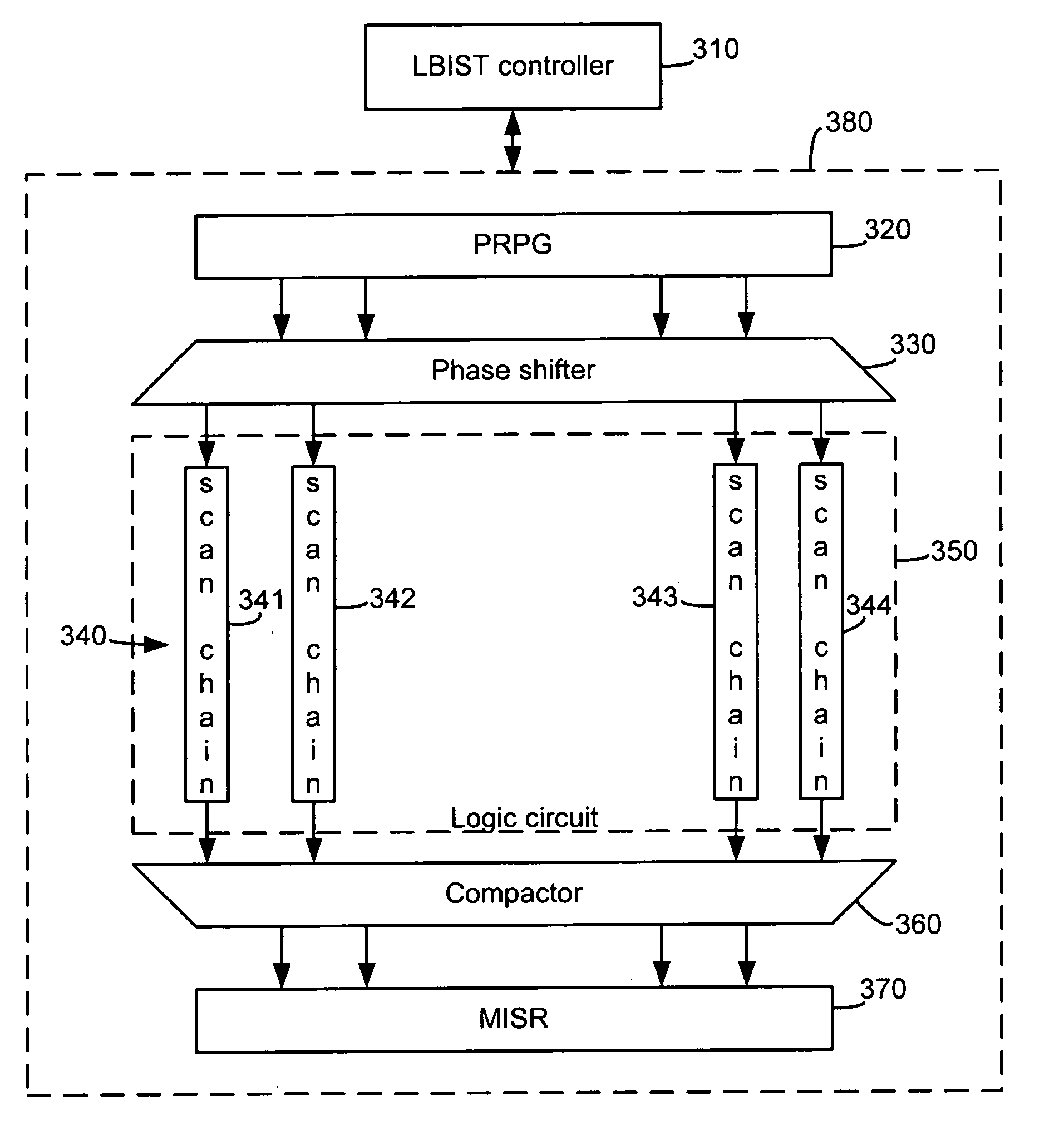
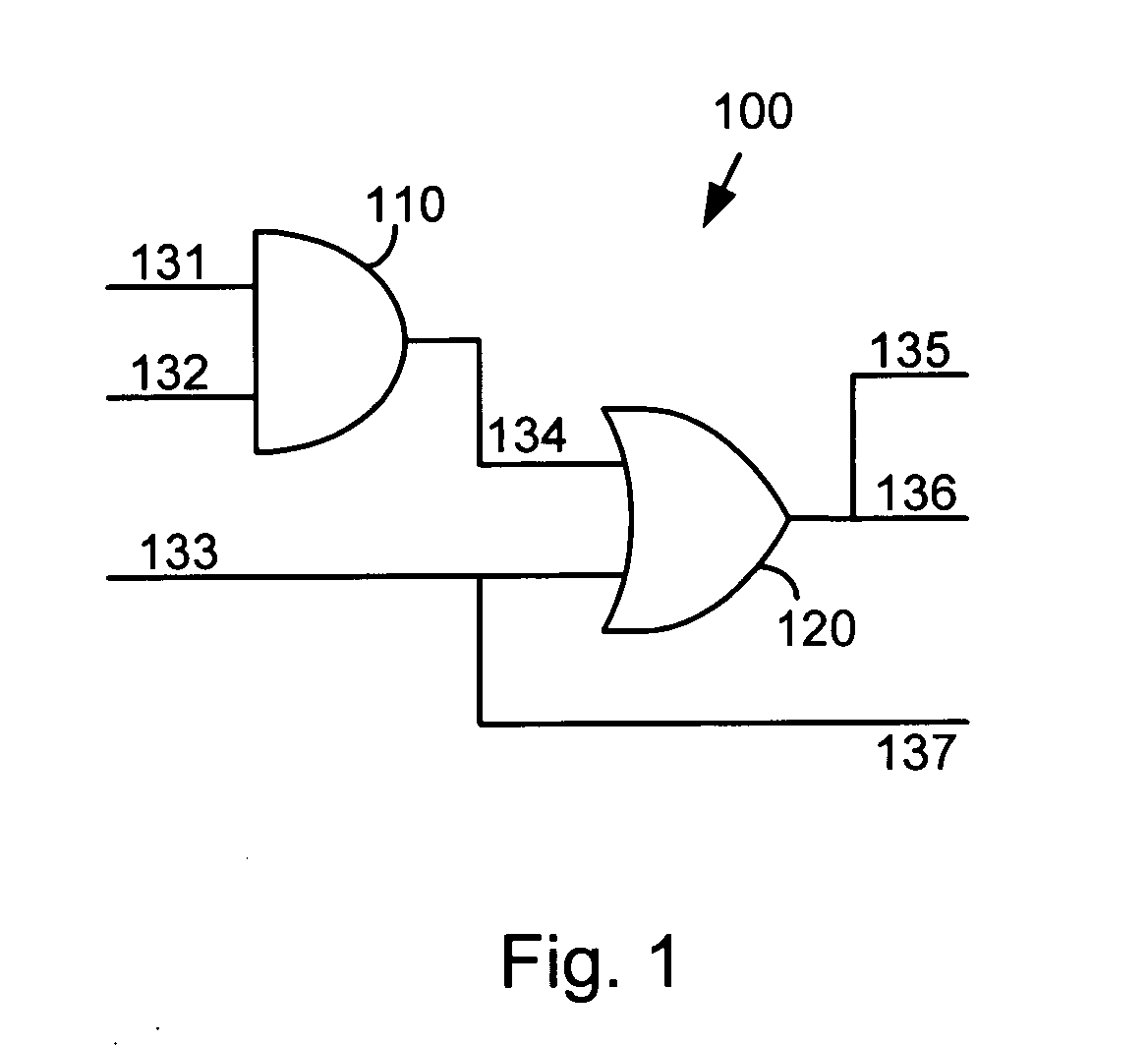
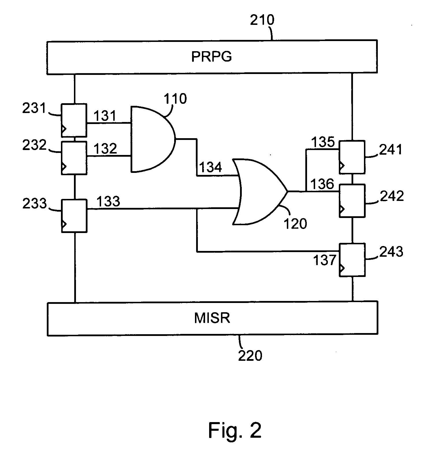
[0032] In one embodiment, a method is implemented in an integrated circuit which incorporates components for a logic-built-in-self-test, or LBIST. The LBIST components can include a plurality of scan chains interposed between levels of the functional logic of the circuit under test so that data in one of the scan chains propagates through a level of functional logic to a subsequent scan latch, and potentially through one or more additional levels of functional logic and corresponding subsequent sca...


PUM


Abstract

Systems and methods for improved performance of built-in-self-tests (BISTs) in integrated circuits, where variability is introduced into the self tests to improve the coverage of the tests. In one embodiment, an LBIST system includes scan chains interposed between levels of functional logic in a circuit under test. An exemplary method includes the steps of, for each of one or more initial scan chains, filling the initial scan chains with data comprising a pseudorandom pattern of bits, determining a number of levels of functional circuitry and corresponding subsequent scan chains through which to propagate the data and propagating the data from the initial scan chains through the determined number of levels of functional circuitry and corresponding subsequent scan chains. The number of levels of circuitry through which data is propagated is varied from one test cycle to another based upon a pseudorandom input signal.

Description

BACKGROUND OF THE INVENTION [0001] 1. Related Art [0002] Digital devices are becoming increasingly complex. As the complexity of these devices increases, there are more and more chances for defects that may impair or impede proper operation of the devices. The testing of these devices is therefore becoming progressively more important. [0003] There are various stages in the life cycle of a device in which testing is important. For example, testing is important in the design of the device, in the manufacturing of the device, and in the operation of the device. At the design stage, testing is intended to verify the design of the device and to identify flaws in the design. Testing may be performed at the architectural level and RTL levels using high level languages or some for of hardware description language (HDL) to simulate the functionality of the device. Simulation testing may also be used to test the gate level design of the device. Testing during the manufacturing of the device ...

Claims


Application Information

Patent Timeline
Patent Type & Authority Applications(United States)
IPC IPC(8): G01R31/28G01R31/3183G01R31/3185H01L21/822H01L27/04H03K3/84H03K19/00
CPCG01R31/318385G01R31/318566G01R31/318536
Inventor KIRYU, NAOKIBUSHARD, LOUIS B.
Owner IBM CORP
Why Eureka
Try Eureka