Plasma processing apparatus

a processing apparatus and plasma technology, applied in the direction of chemical vapor deposition coating, coating, electric discharge tube, etc., can solve the problems of increasing the impedance and loss of a high frequency power supplied to generate plasma, and affecting the quality of plasma generated. , to achieve the effect of stably obtaining a high-quality wafer

Inactive Publication Date: 2005-06-30
TOKYO ELECTRON LTD
View PDF1 Cites 36 Cited by
  • Summary
  • Abstract
  • Description
  • Claims
  • Application Information

AI Technical Summary

Benefits of technology

[0015] It is, therefore, a first object of the present invention to provid...

Problems solved by technology

However, the plasma processing apparatus incorporating the plurality of structures in the electrode housing suffers from various problems as follows.
First, a structure installed inside the electrode housing disturbs a high frequency electromagnetic field inside the outer conductor and, as a consequence, the symmetry of generated plasma is broken.
Further, since the electrode housing and the matching device has their respective housings, a return path of the high frequency power is lengthened, which results in an increase of impedance and loss of a high frequency power supplied to generate a plasma.
Furthermore, when a plurality of structures is installed in the electrode housing, it becomes difficult to secure ...

Method used


Image

  • Plasma processing apparatus
  • Plasma processing apparatus
  • Plasma processing apparatus

Examples


first preferred embodiment

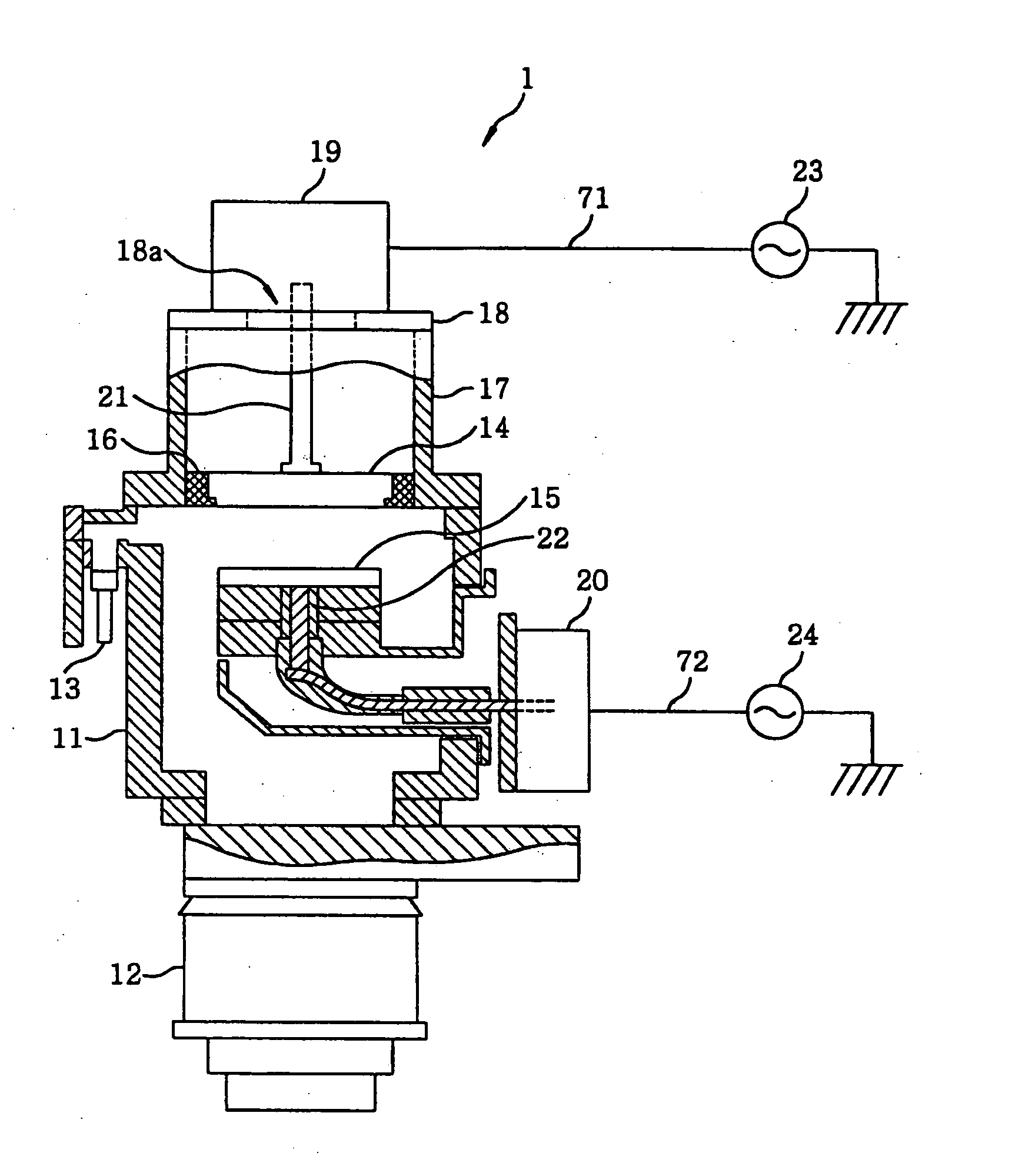
[0036] A plasma CVD apparatus in accordance with a first embodiment has a configuration in which a high frequency electromagnetic field formed inside an electrode housing is not disturbed by a structure installed inside the electrode housing, which serves to support an upper electrode.

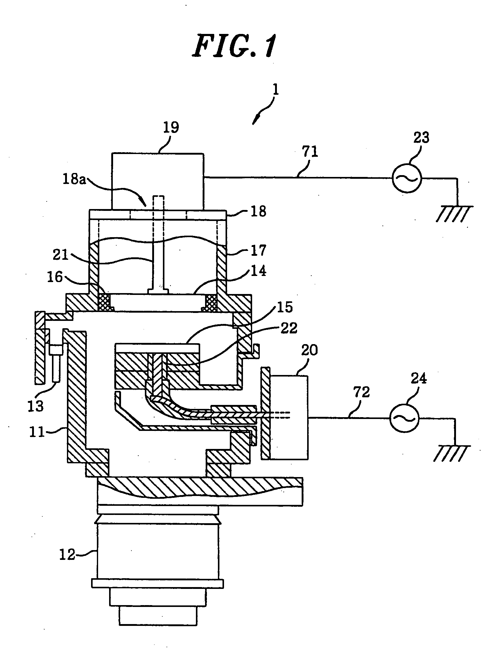
[0037] Referring to FIG. 1, there is illustrated a configuration of a plasma CVD apparatus 1 in accordance with the first preferred embodiment.

[0038] The plasma CVD apparatus 1 is a so-called parallel plate type plasma processing apparatus including an upper and a lower electrode placed to face each other in parallel, and forms, e.g., a SiOF film on a surface of a semiconductor wafer (hereinafter referred to as a wafer) employed as an object to be processed.

[0039] The plasma CVD apparatus 1 includes a vacuum vessel (chamber) 11 and a pump 12.

[0040] A turbo molecular pump is employed as the pump 12, for example. The pump 12 exhausts a gas from the vacuum vessel 11 to thereby produce a depressurized ...

second preferred embodiment

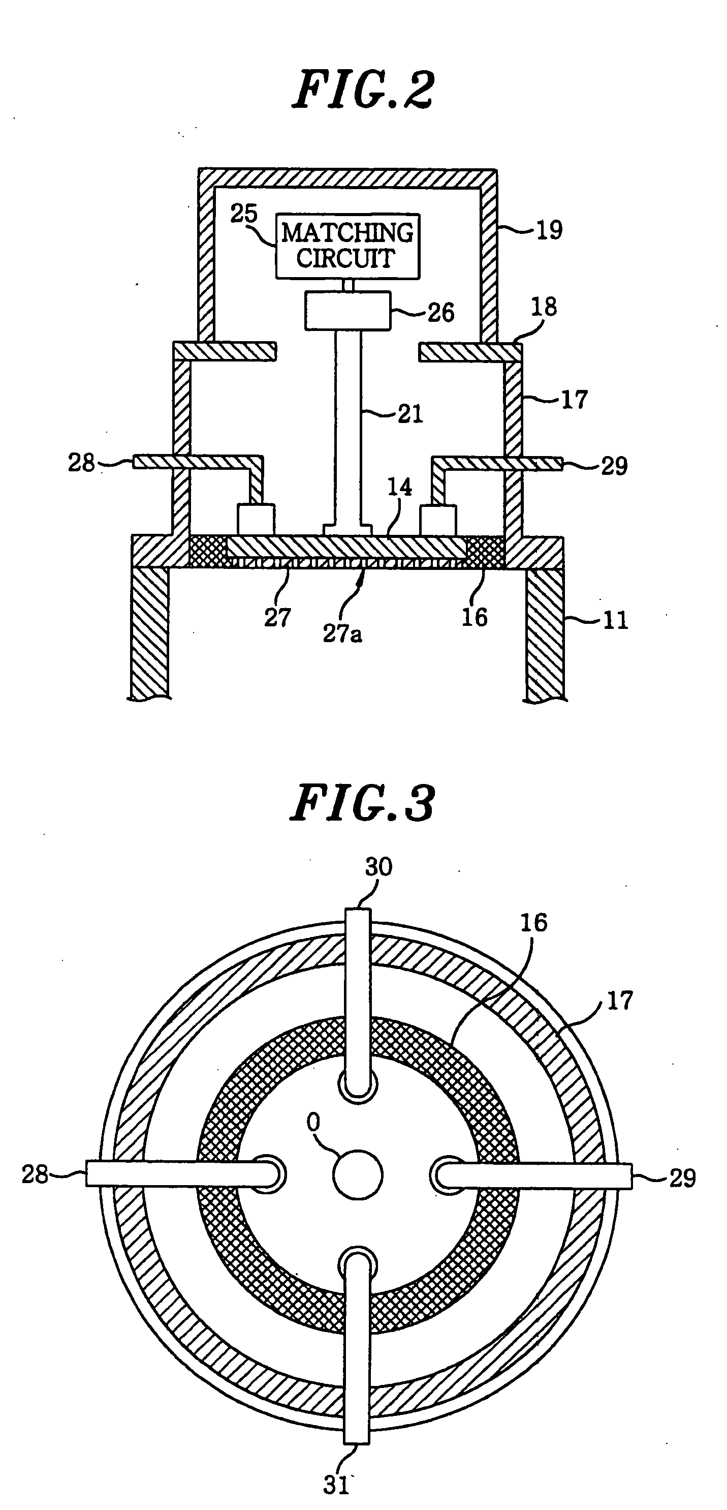
[0075] A plasma CVD apparatus 1 in accordance with a second preferred embodiment is configured to have a shorter return path of a high frequency power applied to an upper electrode 14 in order to suppress a power loss.

[0076]FIG. 4 shows the configuration of the plasma CVD apparatus 1 in accordance with the second preferred embodiment.

[0077] In the plasma CVD apparatus 1 in accordance with the second preferred embodiment, a matching device 19 does not have a conventionally employed bottom plate and a ceiling plate 18 of an enclosure 17 also serves as the bottom plate of the matching device 19 instead.

[0078] As shown in FIG. 5, a groove 17b is formed on an enclosure 17's end surface 17a to be attached to the ceiling plate 18. An elastic gasket 42 for preventing a leakage of the high frequency is disposed in the groove 17b. Once the enclosure 17 and the ceiling plate 18 are tightly fastened by screws or the like, the gasket 42 is deformed to thereby seal the gap between the enclosur...

third preferred embodiment

[0083] In a plasma CVD apparatus 1 in accordance with a third preferred embodiment, a gas supply tube 28, which is one of various structures installed in an enclosure 17, is utilized as a coil element in order to secure installation places for other structures therein.

[0084] As shown in FIG. 8, a high frequency circuit 50 is installed inside the enclosure 17. As will be described hereinbelow, the gas supply tube 28 serving as the coil element constitutes the high frequency circuit 50.

[0085] In the third preferred embodiment, a high frequency voltage supplied from the high frequency oscillator 23 is supplied to the upper electrode 14 with a DC voltage superposed thereon.

[0086] As shown in FIG. 9A, one end of the gas supply tube 28 is connected to the upper electrode 14 while the other end thereof is coupled to the enclosure 17 via a dielectric 51. The gas supply tube 28 is formed of a metal (conductor) and is wound in a coil shape. The dielectric 51 isolates the gas supply tube 28...


PUM

PropertyMeasurementUnit
Poweraaaaaaaaaa
Structureaaaaaaaaaa
Shapeaaaaaaaaaa

Abstract

A plasma processing apparatus includes a chamber 11 for confining a plasma therein; an electrode 14 to which a power for use in generating the plasma is applied; a power supply 23 for supplying the power; an inner conductor 21 for supplying the power from the power supply 23 to the electrode 14; and an outer conductor 17 surrounding the inner conductor. Each of the chamber 11, the inner conductor 21 and the outer conductor 17 has a shape symmetrical with respect to a central axis which passes through a center of the electrode 14 and is perpendicular to the electrode 14. Further, structures 28, 29, 30 and 31 are symmetrically provided with respect to the central axis in the outer conductor 17, and at least one of the structures is a dummy structure 29 having a same shape as that of one of the other structures.

Description

[0001] This application is a Continuation Application of PCT International Application No. PCT / JP03 / 08494 filed on Jul. 3, 2003, which designated the United States.FIELD OF THE INVENTION [0002] The present invention relates to a plasma processing apparatus. BACKGROUND OF THE INVENTION [0003] A plasma processing apparatus is employed to perform a predetermined processing on a semiconductor substrate, a liquid crystal substrate or the like, by using a plasma. A plasma etching apparatus for performing an etching processing on a substrate and a plasma CVD (chemical vapor deposition) apparatus for performing a CVD processing on a substrate are examples of such plasma processing apparatuses. Among various plasma processing apparatuses, a parallel plate type apparatus is widely employed due to its advantages that it has a relatively simple structure and is capable of executing a uniform processing. [0004] The parallel plate type plasma processing apparatus includes a vacuum vessel (chamber...

Claims


Application Information

Patent Timeline
IPC IPC(8): C23C16/509C23F1/00H01J37/32H01L21/306
CPCC23C16/5096H01J2237/3323H01J37/32082
Inventor HIGASHIURA, TSUTOMU
Owner TOKYO ELECTRON LTD
Why Eureka
Try Eureka