Methods of fabricating bipolar transistor

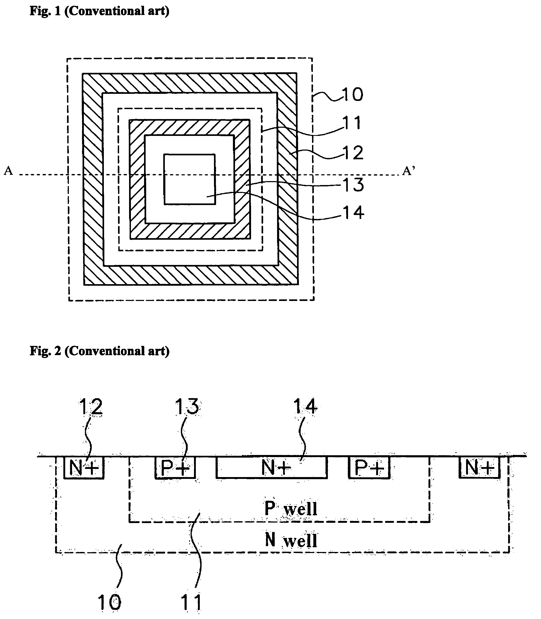
a technology of bipolar transistors and manufacturing methods, which is applied in the direction of transistors, semiconductor devices, electrical equipment, etc., can solve the problems of large manufacturing process difficulties, large size of single chips, and difficulty in realizing transistors with high amplification gains, so as to and reduce the size of the device.

Inactive Publication Date: 2005-06-30
DONGBU ELECTRONICS CO LTD
View PDF16 Cites 0 Cited by
  • Summary
  • Abstract
  • Description
  • Claims
  • Application Information

AI Technical Summary

Benefits of technology

[0011] An object of the present invention is to provide a bipolar transistor and method of manufacturing the same which provides both a high amplification factor and a high current driving force.
[0012] Further objects of the present invention include minimizing a device area by forming the diffusion layer of an emitter and a collector in a device isolation trench (e.g., in the trench sidewalls and / or bottom), and providing a deep impurity diffusion layer (enabled by using the device isolation structure, without necessarily using a high temperature diffusion process).

Problems solved by technology

On the other hand, as the manufacturing processes of memory products and logic products are simultaneously performed, the size of the single chip is getting larger and, therefore, there are a lot of difficulties in conducting the manufacturing process.
Therefore, it is difficult to realize the transistor that has a high amplification gain.
Although the existing method of fabricating the bipolar transistor as described above integrates both the memory and the logic as a semiconductor device into a single chip and in a single process, it is difficult to make a transistor that has a high amplification gain because of the depth of well, and to form both the emitter and the collector that have deep junction depth because of limitations on the source / drain diffusion layer that are formed in the memory transistors at the same time [?].
Therefore, a direct current amplification factor (hfe) and / or the implantation efficiency of holes is low.

Method used


Image

  • Methods of fabricating bipolar transistor
  • Methods of fabricating bipolar transistor
  • Methods of fabricating bipolar transistor

Examples


Embodiment Construction

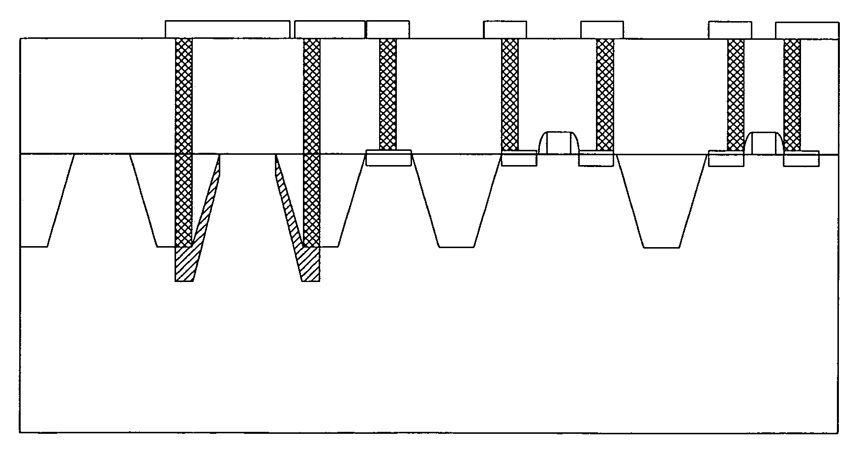
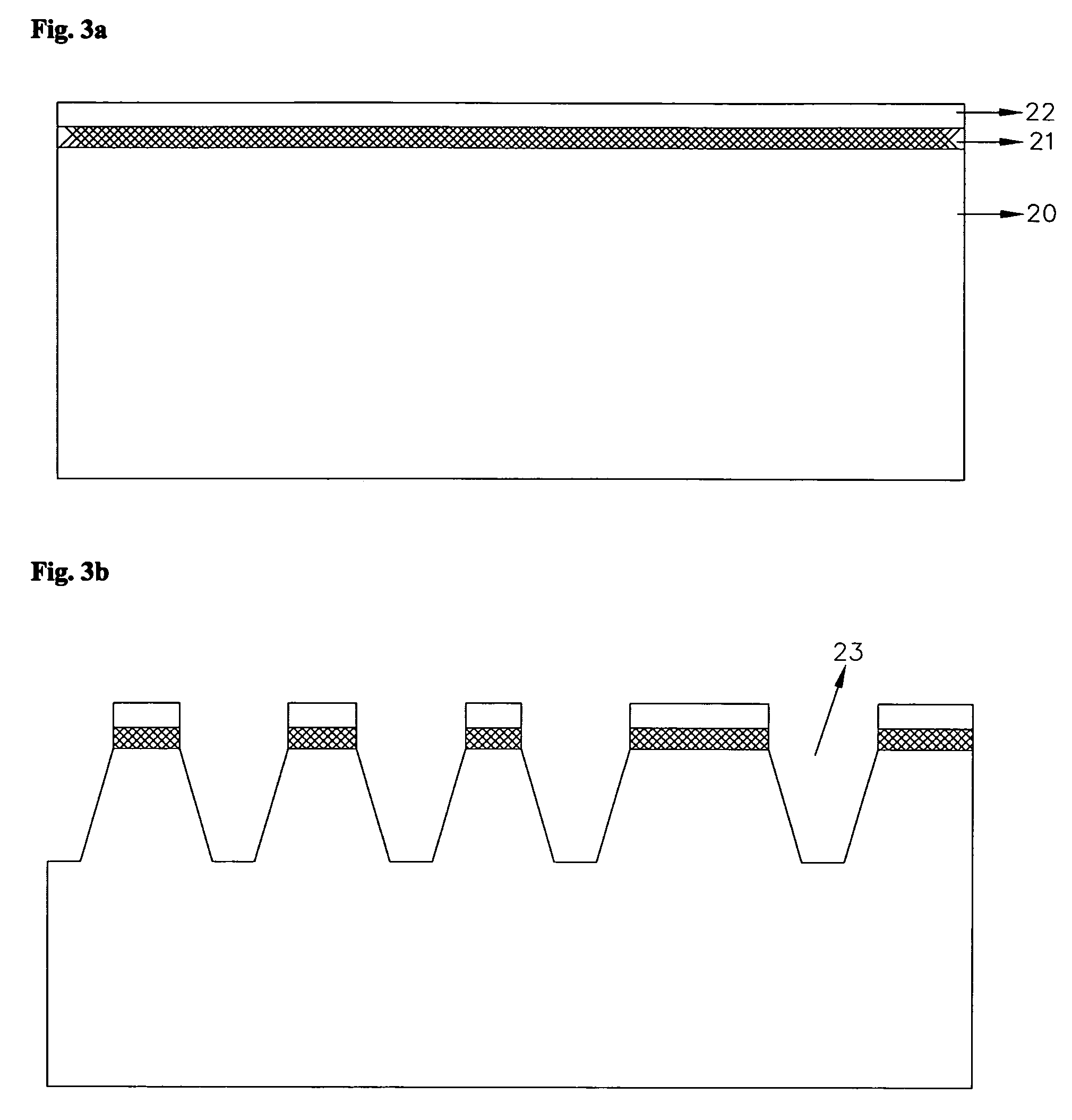
[0019] Reference will now be made in detail to the preferred embodiments of the present invention, examples of which are illustrated in the accompanying drawings, in which FIG. 3a through FIG. 3d are cross-sectional views illustrating example processes of fabricating the bipolar transistor according to an embodiment of the present invention.

[0020] Referring to FIG. 3a, a buffer layer 21 and a nitride layer 22 (not drawn to scale) are successively formed on the upper part of a semiconductor substrate 20. First, buffer layer 21 may comprise a silicon oxide layer grown to a thickness of from 50 Å to 150 Å. Then, a silicon nitride layer is deposited thereon, having a thickness of from 1000 Å to 1 500 Å. This buffer layer works as a buffer to reduce the stress exerted by the nitride layer, and the nitride layer works as an polish or etch stop layer during a CMP (Chemical Mechanical Polishing) process for a planarization of a subsequently formed surface.

[0021] Referring to FIG. 3b, one ...


PUM


Abstract

A bipolar transistor and method of fabricating the same is disclosed. Particularly, a bipolar transistor may have an emitter and a collector diffusion layer in the sidewalls and the bottom of a device isolation trench. A method includes the steps of: forming a device isolation trench in a substrate; forming a photoresist pattern and implanting ions into the sidewalls and the bottom of the trench to form an emitter and a collector; removing the photoresist pattern; and filling the trench with an insulation layer to form the device isolation structure. Accordingly, the transistor and method can minimize device area by forming the diffusion layer of an emitter and a collector in the sidewalls and the bottom of the trench, and can provide a deep impurity diffusion layer without a high temperature diffusion process. In addition, the transistor and method can provide both a high amplification factor and a high current driving force.

Description

BACKGROUND OF THE INVENTION [0001] 1. Field of the Invention [0002] The present invention relates to a bipolar transistor and a method of fabricating the same, and more particularly, to a bipolar transistor having an emitter and a collector diffusion layer in the sidewalls and the bottom of a device isolation trench and a method of fabricating the same. [0003] 2. Background of the Related Art [0004] Due to a great interest in a composite semiconductor, whose memory and logic are formed within a single chip, its usage is increasing. Because the composite semiconductor device can integrate memory and logic into a single chip and manufacture the same in a single process, it can operate faster and use less electric power than existing combinations of chips without any substantial change of design. [0005] On the other hand, as the manufacturing processes of memory products and logic products are simultaneously performed, the size of the single chip is getting larger and, therefore, there...

Claims


Application Information

Patent Timeline
Patent Type & Authority Applications(United States)
IPC IPC(8): H01L21/331H01L21/8222H01L29/73
CPCH01L29/66272H01L21/8222H01L29/73
Inventor SONG, YOO SEON
Owner DONGBU ELECTRONICS CO LTD
Why Eureka
Try Eureka