Laser beam pattern mask and crystallization method using the same

a laser beam and pattern technology, applied in the field of laser beam pattern mask and crystallization method, can solve the problems of inability to provide homogenous grains, inability to provide high heat resistance of high-temperature polysilicon, and inability to meet the requirements of high-temperature polysilicon process, etc., to achieve enhanced crystallization characteristics of beam overlap area

Active Publication Date: 2005-06-30
LG DISPLAY CO LTD
View PDF16 Cites 67 Cited by
  • Summary
  • Abstract
  • Description
  • Claims
  • Application Information

AI Technical Summary

Benefits of technology

[0036] An object of the present invention is to provide a laser beam pattern mask and crystallization method using the same, by which crystallization characteristics of a beam overlap area are enhanced.

Problems solved by technology

Hence, the high-temperature polysilicon process needs an expensive quartz substrate having high heat resistance.
A polysilicon film formed by the high-temperature process shows low-grade crystalline properties, such as high surface roughness, fine grain size, and the like, thereby being inferior to polysilicon formed by the low-temperature process in terms of device operation characteristics.
Yet, the second region fails to provide homogenous grains.
Yet, a plurality of grain boundaries of polysilicon works as obstacles against a current flow, thereby inhibiting the production of a reliable thin film transistor device.
A colliding current and degradation caused by collision between electrons within a plurality of the grains breaks down into an insulator, which results in product failure.

Method used


Image

  • Laser beam pattern mask and crystallization method using the same
  • Laser beam pattern mask and crystallization method using the same
  • Laser beam pattern mask and crystallization method using the same

Examples


first embodiment

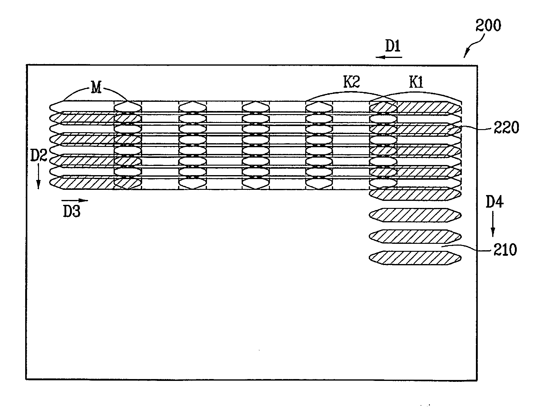
[0064]FIG. 10 is a process layout of a crystallization sequence using the laser beam pattern mask in FIG. 8. Referring to FIG. 10, a crystallization method using a laser beam pattern mask according to the present invention includes the following steps.

[0065] First, a substrate 200 having an amorphous silicon layer 210 deposited thereon is prepared. The substrate 200 is fixed onto a stage (not shown in the drawing). A laser beam pattern mask is prepared. The laser beam pattern mask (‘100’ in FIG. 8) includes a plurality of transmitting parts 110 at predetermined intervals. Each of the transmitting parts includes a central portion and a pair of edge portions provided to both sides of the central portion, respectively. The central portion can be rectangular. Each of the edge portions has a substantially triangular shape defined by a virtual boundary line with the central portion, an upper outside tilted at an acute angle from an upper end of the virtual boundary line, and a lower outsi...

second embodiment

[0076]FIG. 13 is a process layout of a crystallization sequence using the laser beam pattern mask in FIG. 12. Referring to FIG. 13, a crystallization method using a laser beam pattern mask according to the present invention includes the following steps.

[0077] First, a substrate 200 having an amorphous silicon layer 210 deposited thereon is prepared. Next, the substrate 200 is fixed onto a stage (not shown in the drawing). A laser beam pattern mask is prepared like that shown in FIG. 12. The laser beam pattern mask 150 includes a plurality of first transmitting parts ‘D’ and a plurality of second transmitting parts ‘E’ having the same shapes of the first transmitting parts ‘D’. Each of the first transmitting parts ‘D’ includes a central portion and a pair of edge portions provided to both sides of the central portion, respectively. Each of the edge portions has a substantially triangular shape defined by a virtual boundary line with the central portion, an upper outside tilted at an ...


PUM

PropertyMeasurementUnit
acute angleaaaaaaaaaa
angleaaaaaaaaaa
vertical lengthaaaaaaaaaa

Abstract

A laser beam pattern mask includes at least one or more transmitting parts, each transmitting part having a central portion and a pair of edge portions provided to both sides of the central portion, each having a substantially triangular shape defined by a virtual boundary line between the central portion and the corresponding edge portion, an upper outside extending from an upper end of the boundary line at an acute angle, and a lower outside extending from a lower end of the boundary line at the acute angle to meet the upper outside at a rounded corner.

Description

[0001] This application claims the benefit of the Korean Application No. P2003-97585 filed on Dec. 26, 2003, which is hereby incorporated by reference. BACKGROUND OF THE INVENTION [0002] 1. Field of the Invention [0003] The present invention relates to silicon crystallization, and more particularly, to a laser beam pattern mask and crystallization method using the same. [0004] 2. Discussion of the Related Art [0005] As an information society develops, the demand for a visual display is rising in various ways. A variety of flat display devices have been designed to meet such a demand. Many efforts are now being made to further develop flat display devices, such as a liquid crystal display (LCD) device, plasma display panel (PDP), electroluminescent display (ELD), and vacuum fluorescent display (VFD). Some of these flat display devices are already in use in various types of equipment. [0006] When replacing CRT (cathode ray tube), LCD provides excellent features including excellent ima...

Claims


Application Information

Patent Timeline
Patent Type & Authority Applications(United States)
IPC IPC(8): G02F1/13B23K26/06G03F1/14H01L21/20H01L21/77H01L21/84
CPCB23K26/0656H01L27/1285H01L21/2026G03F1/14B23K26/066G03F1/50H01L21/02686H01L21/02532H01L21/0268H01L21/02691G02F1/13
Inventor JUNG, YUN HO
Owner LG DISPLAY CO LTD
Why Eureka
Try Eureka